![]()
NEW CLICK HERE FOR AMAZON PRIME!
NEW CLICK HERE TO SEND US A GIFT! A COOL IDEA TO HELP US FOR HELPING YOU!


|


|


XTAL HOW TO PAGE JUST A FEW THINGS
|
Practical considerations, helpful definitions of terms and useful explanations of some concepts used in this Site
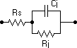
1. An explanation as to why some diodes that work well in the Broadcast Band cause low sensitivity and selectivity when used at Short Waves: The parasitic (approximately fixed) series resistance Rs of a diode is in series with the parallel active elements. The nonlinear active elements are the junction resistance Rj, which is a function of current through the diode, and the junction capacitance Cj, which is a function of the voltage across it.
The nonlinear junction resistance effect is what we use to get
detection. The nonlinear capacitance effect is used when the diode
is designed to be a voltage variable capacitor (a varactor diode).
The parasitic series resistance of some 1N34 diodes can be pretty high, and in series with the junction capacitance, make that capacitance have a rather low Q at high frequencies. This capacitance is, in a crystal radio set, effectively in parallel with the RF tank. The tank usually has a small value tuning capacitor itself, so the overall tank circuit Q is reduced at high frequencies. This is the main reason why diodes having large values for Rs and CJ perform poorly at high frequencies. 2. An explanation of the meaning and use of dB and dBm: In the acronym dBm, "d" means one-tenth. "B" refers to the Bel and is named after Alexander Graham Bell. The Bel is used to express the ratio of two powers, say (Output Power)/(Input Power). Let's call this power ratio "(pr)". Mathematically, a power ratio, expressed in Bels, is equal to the logarithm of the ratio of the two powers. B=log (pr). If the two powers are equal, the power ratio expressed in Bels is 0 B. This is because the log of one is zero. Another illustration: Assume that the power ratio is twenty. (Pr)=20. The logarithm of 20 is about 1.3. This power ratio in Bels is 1.3 B. One decibel is equal to 0.1 Bel. That is, 10 dB=1 B. If we express the two power ratios mentioned above (1 and 20) in dB, we get 0 dB and about 13 dB. So far, we have seen that the decibel is used to express the ratio of two powers, it is not a measure of a power level itself. A convenient way to express an actual power level using dB is to use a standard implied reference power for one of the powers. dBW does this. It expresses the ratio of a power to the reference power (One Watt in this case). dBm uses a reference power of one milliwatt. A power level of, say 100 milliwatts, can be said to be a power level of +20 dBm (twenty dB above one milliwatt). Why? (100 milliwatts)/(1 milliwatt)=100. The logarithm of 100 is 2. 10 times 2 equals 20. The convenient thing about using dB comes from a property of logarithms: The logarithm of the product of two numbers is equal to the sum of the logarithm of each number, taken separately. An illustration: If one has a power source of, say 2.5 mW and amplifies it through an amplifier having a power gain of, say 80 times, the output power is 2.5 X 80=200 mW. 2.5 mW expressed in dBm is +4 about dBm. A power gain of 80 times is about +19 dB. The output power is 4+19=+23 dBm. 3. Maximum Available Power: If one has a voltage source Vs with an inaccessible internal resistance Rs, the load resistance to which the most power (Pa) can be delivered is equal to Rs. Pa is called the 'maximum available power' from the source Vs, Rs. Any load resistance other than one equal to the source resistance, Rs, will absorb less power. This applies whether the voltage is DC or AC (RMS). The formula for power absorbed in a resistance is "voltage-squared divided by resistance". In the impedance matched condition, because of the 2 to 1 voltage division between the source resistance and load resistance, one-half of the internal voltage Vs will be lost across the internal source resistance. The other half will appear across the load resistance. The actual power available to the load will be, as indicated in the preceding relation: Pa = [(Vs/2)^2]/Rs = (Vs^2)/(4*Rs). Again, in the impedance matched condition, the total power delivered to the series combination of source and load resistance is divided up into two halves. One half is unavoidably lost in the internal source resistance. The other half is delivered as "useful output power" to the load resistance. The 'maximum available power' approach is useful when measuring the insertion power-loss of two-port devices such as transformers, amplifiers and crystal radio sets, which may not exhibit an input or output impedance that is matched to the power source. The input impedance may be, in fact a combination of resistive and reactive components. If the Vs,Rs source is connected to a resistive load (Ro) of value equal to Rs ohms, it will receive and dissipate a power of Pa Watts. This is the maximum available power from the Vs, Rs source, so we can say we have a 'no loss' situation. Now, assume that a transformer or other two-port device is inserted between the Vs,Rs source and Ro, and that an output voltage Vo is developed across Ro. The output power is (Vo^2)/Ro. The 'insertion power loss' can now be calculated. It is: 10*log (output power)/(maximum available input power) dB. After substituting terms, the equation becomes: Insertion power loss =10*log [(Vo/Vs)^2)*(4*Rs/Ro)] dB. If the input voltage is referred to by its peak value (Vsp) as it is in a SPICE simulation, instead of by its RMS value, the equation changes. The RMS voltage of a sine wave is equal to the peak value of that wave divided by the "square root of 2". Since the power equation squares the voltage, the equation for the 'available input power' changes to Pa = (Vsp^2)/(8Rs). 4. Diode Saturation Current and Ideality Factor: Saturation current is abbreviated as Is in all of these articles. Assume that one connects a DC voltage source to a diode with the polarity of the voltage source such as to bias the diode in the back direction. Increase the voltage from zero. If the diode obeys the classic Shockley ideal equation exactly, the current will start increasing, but the increase will flatten out to a value called the saturation current as the voltage is further increased. That is, as the voltage is increased, the current will asymptotically approach the saturation current for that diode. A real world diode has several mechanisms that cause the current to actually keep increasing somewhat and not flatten out as the back direction voltage is further increased. Diode manufacturers characterize this as reverse breakdown and specify that the back current will be less than a specified value, say 10 uA at a specified voltage, say 30 V, called the reverse breakdown voltage. BTW there are other causes of excessive reverse current that are collectively referred to as reverse bias excess leakage current. Some diodes have a sharp, controlled increase in reverse current at a specified voltage. These diodes are called Zener diodes. Diode Saturation Current is a very important SPICE parameter that, along with the diode Ideality Factor, n determines the actual diode current when it is forward biased by at particular DC Voltage. Id=Is*(e^(Vd/(0.026*n)-1) at room temperature. This expression ignores the effect of the parasitic series resistance of the diode because it has little effect on the operation of crystal radio sets at the low currents usually encountered. Here Id is the diode current, e is the base of the natural logarithms (2.7183...), ^ means raise the preceding symbol to the power of the expression that follows (Sometimes e^ is written 'exp'), * means multiply the preceding and following symbols, VD is the voltage across the diode and n equals the "Ideality factor" of the diode. At low signal levels, most detector diodes have an n of between 1.05 and 1.2). The lower the value of n, the higher will be the weak signal sensitivity. One can see that Is is a scaling factor for the actual curve generated by the factor (e^(VD/(0.026*n)-1). Diode ideality factor (n): The value of n affects the low signal level sensitivity of a diode detector and its RF and audio resistance values. n can vary between 1.0 and 2.0. The higher the value of n, the worse the low signal level detector sensitivity. The low signal level RF and audio resistances of a diode detector vary directly with the value of n. Schottky diodes usually have a value of n between 1.03 and 1.10. Good germanium diodes have an n of about 1.07 to 1.14 when detecting weak signals. Silicon p-n junction diodes such as the 1N914 have values of n of about 1.8 at low currents and therefore have a lower potential sensitivity as diode detectors than Schottky and germanium point contact diodes. The value of n in Schottky diodes seems to be approximately constant over the full range of currents and voltages encountered in crystal radio set operation, but varies with diode current in silicon pn junction and germanium point contact diodes. A way of thinking about n is to consider it as a factor that effectively reduces the applied signal voltage to a diode detector compared to the case of using an ideal diode having an n of 1.0. Less applied signal, of course, results in less detected output. Here are a few bits of information relative to diodes: Typically, if a diode is biased at 0.0282*n volts in the forward direction, it will pass a current of 2 times its Is. If it is biased at 0.0182*n volts in the reverse direction, it will pass a current of 0.5 times its Is. If a diode is biased at 0.0616*n volts in the forward direction, it will pass a current of 10 times its Is. If it is biased at -0.0592*n volts, it will pass a current of -0.9 times its Is. These values are predicted from the classic Shockley equation. In the real world, reverse current can depart substantially from values predicted by the equation because of effects not modeled (the reverse current becomes higher). Gold bonded germanium diodes usually depart somewhat from the predicted values when operated in the forward direction. The effect appears as an increase of Is when measurements are made at currents above about 6 times the low-current Is. Values of Is and n determine the location of the apparent 'knee" on a linear graph of the diode forward current vs. forward voltage. See Article #7. An easy way to estimate the approximate value of Is can be found in Article #4, section 2. A method of measuring Is and n is given in Article #16. If one connects two identical diodes in parallel, the combo will behave as a single diode having twice the Is, and the same n as one of them. If one connects two identical diodes in series, the combo will behave as a single diode having twice the n and the same Is as one of them. This connection results in a diode having 3 dB less potential weak signal output than one of the diodes by itself. 5. Explanation of why, in a diode detector, and by how much, the RF input resistance and audio output resistances change as a function of input signal power. Consider first, a diode detector that is well impedance-matched both at its input and its output when driven by a very low power RF input signal. There will then exist an appreciable power loss in the detector. (The audio output power will be appreciably less than the input power.). The input and output impedances of the detector will approximately equal each other and approach: Rd = 0.026*n/Is. See part 3 above for a definition of terms. For this illustration, let the diode have an Is of 38 nA and an n of 1.02. Rd will be 700k Ohms. The well impedance-matched condition will hold if the input power is raised from a low value, but only up to a point. After that , the match will start to deteriorate. At an input power about 15 dB above that of the square-law-linear crossover point, the match will have deteriorated to a VSWR of about 1.5:1 (VSWR = Voltage Standing Wave Ratio.). A further increase of input signal power will result in a further increase of VSWR. This means that the input and output resistances of the detector have changed from their previously matched values. The input resistance of the diode detector decreased from the value obtained in the well impedance matched low power level situation. The output resistance increased. The reason for this change is that a new law now governs input and output resistance when a diode detector is operated at a high enough power level to result in a low detector insertion power loss. It now operates as a peak detector. The rule here is that the CW RF input resistance of a diode peak detector approaches ½ the value of its output load resistance. Also, the audio output resistance approaches 2 times the value of the input AC source resistance. Further, since the detector is now a peak detector, the DC output voltage is the "square root of 2" times larger than of the applied input RF RMS voltage. (It's equal to the peak value of that voltage). These existence of these relationships is necessary so that in an ideal peak detector, the output power will equal the input power (No free lunch). Summary: Output DC voltage equals sqrt2 times input RMS voltage. Since the output power must equal the input power, and power equals voltage squared divided by resistance, the output load resistance must equal two times the source resistance, assuming impedance matched conditions prevail. If we were to adjust the input source resistance to, say 495k ohms (reduce it by sqrt2) and the output load resistance to 990k ohms (increase it by sqrt2) by changing the input and output impedance transformation ratios, the insertion loss would become even lower than before the change and the input and output impedance matches would be very much improved (remember we are now dealing with high signal levels). A good compromise impedance match, from one point of view, occurs if one sets the RF source resistance to 0.794*Rd and the audio load resistance to 1.26*Rd. With this setup, theoretically, the impedance match at both input and output remains very good over the range of signals from barely readable to strong enough to produce close to peak detection. A measure of impedance match is "Voltage Reflection Coefficient", and in this case it is always better than 18 dB (VSWR better than 1.3). Excess insertion loss is less than 1/3 dB and selectivity is largely independent of signal level. Information presented in Article #28 shows that, if the diode load resistance is made equal to Rd and the RF source resistance is made equal to Rd/2, the weak signal output of the detector will be about 2 dB greater than if both ports are impedance-matched! There is little benefit when strong signals are received, since both input and output ports become impedance matched. Here is an interesting conceptual view of a high signal level diode detector circuit: Assume that it is driven with a sufficiently high level sine wave voltage so it operates in its peak detection mode, and is loaded with a parallel RC of a sufficiently long time const ant. This detector may be thought of as a low loss impedance transformer with a two-to-one impedance step up from input to output, BUT having an AC input and a DC output, instead of the usual AC input and output. The DC output power will approximately equal the AC input power and the DC output voltage will be about sqrt 2 times the RMS AC input voltage. 5A. A comparison of conventional
half-wave and half-wave voltage-doubling detectors: Here is
some info that may be of interest re conventional half-wave detectors
vs. voltage doubling half-wave detectors when each is terminated with an
output load of Ro. For illustration purposes we will assume the input
voltage to the detector to be 1.0 volt RMS. The RF input resistance of
the detector will be designated as Ri. All diodes have the same Is and
n. It is assumed that good diodes such as a 5082-2835 Schottky, ITT
FO-215 germanium or other are used. The info relates to the RF input
resistance of detectors (it has a large effect upon selectivity) and
their output audio resistance. See Point 4 in this Article for info on
diode Is and n. 1) Conventional half-wave detector operating at a high input signal power level: The detector, in this case, operates as a peak detector. Since it is a passive device, its output power will approximately equal its input power, under impedance-matched conditions. The output DC voltage will approach sqrt2 times the input RMS voltage, since the peak value of a sine wave is sqrt2 times its RMS value. For the input power, (1.0^2)/Ri, to equal the output power, [(1.0*sqrt2)^2]/Ro, the input RF resistance (Ri) must equal 1/2 Ro. That is, Ri=Ro/2. This illustrates the direct interaction between the RF input resistance and output audio resistive load. At high input power levels selectivity drops when the resistive audio output load value is lowered. The audio output resistance of the detector approaches 2 times the RF source resistance driving it. If the diode were an ideal diode, the word "approximately" should be eliminated, and "approaches" should be changed to "becomes" . 2) Conventional half-wave detector operating at a low input signal power level: The detector, in this case, does not operate as a peak detector, and exhibits significant power loss. At low input signal power levels Ri approaches 0.026*n/Is ohms (diode axis-crossing resistance) and becomes independent of the value of Ro. The audio output resistance of the detector approaches the same value as the axis-crossing resistance (see above). 3) Half-wave voltage doubling detector operating at a high input signal power level: The detector, in this case, operates as a peak detector. Since it is a passive device, its output power will approximately equal its input power, under impedance-matched conditions. The output DC voltage will approach 2.0*sqrt2 times the input RMS voltage, since the peak of a 1.0 volt RMS sine wave is sqrt2 times its RMS value. For the input power (1.0^2)/Ri to equal the output power [(1.0*2*sqrt2)^2]/Ro, the input RF resistance (Ri) must equal 1/8 Ro. That is, Ri=Ro/8. This illustrates the direct interaction between the RF input resistance and output audio resistive load. At high input power levels selectivity drops substantially if the output resistive audio load value is lowered. The audio output resistance of the detector approaches 8 times the RF source resistance driving it. This fact is seldom recognized and it may be the cause of some of the problems encountered by those experimenting with doublers. 4) Half-wave voltage doubler operating at a low input signal power level: The detector, in this case, does not operate as a peak detector, and it has significant power loss. At low input signal power levels Ri approaches (0.026*n/Is)/2 ohms and becomes independent of the value of Ro. The audio output resistance of the detector approaches twice the axis-crossing resistance of the diode. 5) Summary: At high input power levels, and with both input and output matched, power loss in both half wave and half wave voltage doubling detectors approaches zero dB. Sound volume should be the same with either detector. At low input power levels both detectors exhibit substantial power loss. I believe, but have not proven, that at low input power levels the doubler has a higher power loss than the straight half wave detector, and should deliver less volume. 6. Some misconceptions regarding Impedance matching and Crystal Radio Sets: To understand the importance of impedance matching, one must first accept the concept of power. A radio station accepts power from the mains and converts some of it to RF power which is radiated into space. This power leaves the transmitting antenna at the speed of light and spreads out as it goes away from the antenna. One can prove that power is radiated by substituting a LED diode for the regular diode, getting physically close enough to the station and then tuning it in. The LED will light up (give off light power), showing that some power is being broadcast and that it can be picked up. Now back at home, if one tunes in the station one gets sound in the headphones. What activates one's hearing system is the power of the perceived sound. BTW, if one gets too much sound power in the ear for a long enough time, the power can be strong enough to break off some of the hair cells in the inner ear and reduce one's hearing sensitivity forever. The theoretical best one can do with a crystal radio set setup is the following: (1) Use an antenna-ground system to pick up as much as possible of the RF power passing through the air in its vicinity . In general, a higher antenna will pick up more power from the passing RF waves than will a lower one. (2) Convert the intelligence carrying AM sideband RF power into audio electrical power. (3) Convert the electrical audio power into sound power and get that power into the ear. There are power losses at each of the three steps and our job is to minimize them in order to get as much of the sideband RF power passing through the vicinity of the antenna (capture area) changed into audio power for our ears. We want all of the "available power" at the antenna-ground system to be absorbed into the crystal radio set then passed on through it to our headphones as sound. However, some of it will be unavoidably lost in the RF tuned circuit. If the input impedance of the crystal radio set is not correctly matched to the impedance of the antenna, some of the RF power hitting the input to the crystal radio set will be reflected back to the antenna-ground system and be lost. An impedance-matched condition occurs when the resistance component of the input impedance of the crystal radio set equals the source resistance component of the impedance of the antenna-ground system. Also, the reactive (inductive or capacitive) component of the impedance of the antenna-ground system must see an opposite reactive (capacitive or inductive) impedance in order to be canceled out. In the impedance-matched condition, all of the maximum available power (See section on "Maximum Available Power" above) intercepted by the antenna-ground system is made available for use in the crystal radio set and none is reflected back towards the antenna to be lost. Now we are at the point where confusion often exists: The voltage concept vs. the power concept. Let's assume that the diode detector has a RF input resistance of 90,000 Ohms. Assume that the antenna-loaded resonant resistance of the tuned circuit driving it is 10,000 Ohms. If one uses voltage concepts only, one might think that this represents a low loss condition. NOT SO! After all, 9/10 of the actual source voltage is actually applied to the detector. If one impedance matches the 10k ohm source RF resistance to the diode 90k ohm RF resistance via RF impedance step-up transformation (maybe connecting the antenna to a tap on the tuned circuit, and leaving the diode on the top), good things happen. (We will assume here that, in the impedance transformation to follow, the ratio of loaded-to-unloaded Q of the tuned circuits is not changed.) For an impedance match, the tuned circuit resonant resistance should be transformed up by 9 times. If this was done by a separate transformer (for ease of understanding) it would have a turns ratio of 1:3, stepping up the equivalent source voltage by 3 times and changing the equivalent source resistance to 90,000 Ohms. What now? Before matching, the diode got 9/10 of the source voltage applied to it. Now it gets 1/2 the new equivalent source voltage (remember the equivalent voltage is 3 times the original source internal voltage). The 1/2 comes from the 2:1 voltage division between the resistance of the equivalent source of 90,000 Ohms and the detector input resistance of 90,000 Ohms. The ratio of the new detector voltage to the old is: 3 times 1/2 divided by 0.9 = 1.67 times. This equates to a 4.44 dB increase in power applied to the detector. If the input signal to the detector is so weak that the detector is operating in the square-law region, the audio output power will increase by 8.88 dB! This is about a doubling of volume. 7. Caution to observe when cutting the leads of a glass Agilent 5082-2835 Schottky diode (or any other glass diode): When it is necessary to cut the leads of a glass packaged diode close to the glass body, use a tool that gives a scissors type of cut. Diagonal cutters give a sudden physical shock to the diode that can damage its electrical performance. This physical shock is greater than one might expect because of the use of plated steel instead of more ductile copper wire. Steel is used, in part, because of its lower heat conductivity, to reduce the possibility of heat damage during soldering. 8. Several different ways to look at a diode detector: A diode detector can be thought of as a mixer, if one thinks of its input signal as consisting of two identical signals of equal power, in phase with each other. It is well known that if a common AM mixer is fed with two signals of frequencies f1 and f2 Hz, most of the output it generates will consist of the second harmonic of each signal and two more signals at other frequencies. One is at the sum frequency (f1+f2) Hz and one at the difference frequency (f1-f2). Additional mixer products can be generated, but they will be weaker than those mentioned and will be neglected in this discussion. In the case of an AM diode detector, we may consider that its input signal of power P Watts is in reality the sum of two equal in-phase signals, each of power P/2 and that there will be four output components, as stated above. They are:
A diode detector can be thought of as a "Black Box". If the DC output impedance of the detector is matched to its load resistor and the AC signal power source of P Watts 'available power' is impedance matched to the input AC impedance of a diode detector, the DC output power can closely approach the 'available power' from the AC source. This gives us another way to look at a detector. It can be considered to be a "Black Box" that changes incident AC power of frequency "f" Hz into output power of frequency zero Hz (DC). This is the detected DC output. 9. Using surface mount components in crystal radio sets: A convenient way to connect to the tiny leads of small surface-mount diode and IC devices is to first solder them to a "Surfboard". Pigtail leads can them be soldered through holes drilled in the Surfboard conducting races for connection to a circuit. A surface mount device such as the OPA-349 integrated circuit (Eight lead SOIC package) can be soldered to a surfboard such as that manufactured by Capital Advanced Technologies ( http://www.capitaladvanced.com ). Their Surfboards #9081 or #9082 are suitable and are available from various distributors such as Alltronics, Digi-Key, etc. Surface mount diodes manufactured using the SOT-23 package can be handled using Surfboard #6103. Diodes using the smaller SOT-323 package can be handled using Surfboard #330003. This includes many Agilent surface mount diodes useful in crystal radio sets. Packages containing multiple diodes exist that use the SOT-363 six lead package. They can be handled using Surfboard #330006. Agilent produces many of their Schottky diodes in dual, triple and quad form in the SOT-363 package. It is recommended that anyone considering using Surfboards visit the above mentioned Website and read "Application Notes" and the "How-to Index". 10. How to modify the tone quality delivered by headphones: It is interesting to note that driving magnetic headphone elements with a high source resistance tends to improve the treble and reduce the bass response, compared to the response when the AC source resistance matches the effective impedance of the elements. Conversely, driving the headphones elements from a low resistance source tends to roll off the treble, and relatively speaking, improve the bass. With piezo ceramic or crystal elements, a high source resistance tends to reduce the treble and improve the bass response, compared to the response where the source resistance matches the effective impedance of the elements. A low source resistance tends to reduce the bass and emphasize the treble. Some piezo elements sound scratchy. This condition can be minimized by driving the elements from a lower resistance source. Here are some practical experimental ways to vary the audio source resistance of a crystal radio set when receiving weak-to-medium-strength signals. A medium strength signal is defined as one at the crossover point between linear to square law operation (LSLCP). See the graphs in Article #15A.
11. Long term resistance drift and frequency dependence of the AC resistance of low power resistors, etc: From my early experience in the manufacturer of Blonder-Tongue products, the following is some insight relative to run-of -the-mill commercial carbon-composition resistors that we used: The process used by the resistor manufacturer is an important factor in the determination of long term resistance drift. Allen-Bradley (A-B) used their 'hot-mold' process, producing a more dense product then did the other manufacturers, as far as I know. The value of this carbon comp. resistor drifts the least, as a rule. Stackpole composition. resistors used their 'cold-mold' process and seem to drift more than do the A-B units. Composition carbon resistors mfg. by the Speer company, using their 'cold-mold' process drift more than the Stackpole resistors, as a rule. The IRC resistors that look like carbon comp. units actually are made by another process. They are called metallized resistors. My impression is that their drift is similar to the of Stackpole resistors. I have found that the IRC resistors usually generate much more low frequency noise when passing a DC current than the others. It seems, as a general rule, that the high value resistors drift more, over time, than the low value ones. The brand of resistor may be guessed by examining the smoothness and shininess of its surface finish, and looking at each end of the resistor to see where the wire exits. Allen Bradley resistors look the best. They have bright color code colors and a smooth shiny finish. At the wire exit point from the body one can usually see the appearance of a small shiny ring embedded in the plastic. Actually, this is part of the lead, shaped to be the contact electrode. Stackpole resistors look next best. They have somewhat duller colors on the color code and the surface is somewhat rougher and less shiny. The wires exit cleanly from the end of the resistor, no ring is visible. The Speer resistors have the dullest color code colors and a rougher surface than the Stackpole's. They usually look as if they have been wax impregnated. At the axial exit points from the body, a small copper colored dot may be seen next to the wire lead. This is actually the end of the lead, which was folded over and back on itself to form the electrode. The IRC so-called carbon comp. resistors can be identified by the visible 'mold-flash' marks on the body and ends. The colors are good, but the body is rough. Their end surfaces are slightly convex, not planar as in the case of the other resistors. Remember, these resistors usually made spec. when new, passed incoming inspection and standard aging tests. Unfortunately, no aging tests could be made that covered the span of many decades. It is interesting to note that the best resistors, from a long term resistance drift point of view turn out to be the AB units. They also cost the most. The Speer units cost the least and the Stackpole's were in between. Ohmite carbon comp resistors I have seen looked like A-B units. A fact of interest that some may not know is this: The AC
resistance of carbon composition resistors, and film resistors, to a
much lesser degree, decrease with increasing frequency (the
Boella Effect). This effect is strongest in high value resistors,
above, say, 22k ohms and above 50 MHz (film resistors). The effect
is noticeable in 500k and 1 meg units at lower frequencies. Low
value resistors having short leads and resistances in the mid 10s to
mid hundreds of ohms are quite free of this effect up through many
hundreds of MHz. A typical graph of the ratio of AC-to-DC
resistance vs frequency, of various values of conventional
commercial axial-lead carbon film type resistors, taken from
a Brell Components catalog is
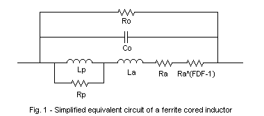
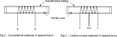
12. The effects from using the contra-wound dual-value inductor configuration in crystal sets as compared to using a conventionally wound inductor, both using capacitive tuning Some quick facts:
See 'The contra-wound tank inductor' in Part 3 of Article #26 and the paragraph after Figs. 2 and 3 in Article #29 for descriptions of two different contra-wound configurations. Discussion: Let us divide the BC band geometrically into two halves: This gives us 520-943 kHz for the low band and 943-1710 kHz as the high band. Assume, for ease of understanding, that the tank inductor for the conventional approach has an inductance of 250 uH. Conventional 250 uH inductor: The whole BC band of 520-1710 kHz can be tuned by a capacitance varying from 374.7 to 34.65 pF. Contra-wound 250/62.5 uH inductor: The low band of 520-943 kHz can be tuned, using the 250 uH series connection, by a capacitance varying from 374.7 to 113.94 pF. The high band of 943-1710 can be tuned, using the 62.5 pF parallel connection, by a capacitance varying from 455.76 to 138.60 pF. For the purposes of this discussion, let us assume that antenna matching (see Part 2 of Article #22) is always adjusted to reflect a fixed shunt resistance of 230k ohms for driving the diode, over the full BC band. 230k ohms is also the RF input resistance of an ITT FO-215 germanium diode when fed a signal power well below its linear-to-square law crossover-point (see Article #10, points 1, 2 and 3 below Fig.1 in Article #15, Article 17A and Article #22). This setting approximates that for minimum insertion power loss (see Article #28). Reduction of insertion power loss at the high end of the BC band (1720 kHz): The total tuning capacitance needed when tuning a conventional 250 uH inductor to 1710 kHz is 39.9 pF. The value needed, using a contra-wound approach is 138.6 pF. One can derive, from data values in Figs. 1 - 4 in Article 28, that the Q of the common 365 pF, non-ceramic insulated variable capacitor (capacitor B), at 1710 kHz comes out as follows:
From Fig. 3 in Article #24 we can see that, at 1710 kHz, the Q of capacitor A, a ceramic-insulated, with silver plated plates capacitor manufactured by Radio Condenser Corporation, or its successor TRW, has a Q of 9800. This is much higher than that of capacitor B when using a conventional 250 uH inductor. Changing to a contra-wound coil while using the easily available capacitor B goes a long way toward a goal of reducing the effect of the variable capacitor on tank Q and loss at the high end of the band. Less selectivity variation and less insertion power loss: Conventional inductor: The 3 dB down RF bandwidth will vary from 3.69 kHz at 520 kHz to 39.9 kHz at 1710 kHz, a variation of 11.6 times . Contra-wound inductor: The 3 dB down RF bandwidth will vary from 3.69 kHz at 520 kHz to 12.15 kHz at 943 kHz in the low band, and from 3.04 kHz at 943 kHz to 9.99 kHz at 1710 kHz in the high band, an overall variation of 4.00 times. This is about 1/4 of the variation experienced when using a conventional inductor. If greater selectivity is needed at the high end of the BC band when using a conventional inductor, antenna coupling must be reduced and/or the diode must be tapped down on the tank to raise the loaded Q. Either approach results in a greater insertion power loss and a weaker or inaudible signal to the phones when tuning stations near the high end of the BC band . The low inductance (parallel connection) of the contra-wound inductor enables a 4 times reduction in bandwidth at 1710 kHz, compared to results with conventional inductor. This reduces the need to tap the diode down on the tank and re-match the antenna when one needs to increase selectivity, as mentioned above. Note:
|
 . A chart providing similar info on carbon composition resistors,
taken from the Radiotron Designer's Handbook, Fourth Edition, page
189 is
. A chart providing similar info on carbon composition resistors,
taken from the Radiotron Designer's Handbook, Fourth Edition, page
189 is
 .
.
Quick introduction:
A crystal radio set may be thought of as the cascaded connection of several basic components.
The Antenna and RF Tuned Circuit will be combined into three components. V1 and R1 represent the antenna induced voltage and resistance, impedance transformed by the tuned circuits and antenna reactance to the series-connected values seen by the diode detector. X1 represents the reactance of the tuned circuit(s) seen at its output terminals. Its impedance is considered to be substantially zero at harmonics of the frequency to which it is tuned. Its impedance is also substantially zero at DC and at Audio frequencies. R2 represents all the losses in the tuned circuits at resonance, as seen by the diode. This is not the conventional way of viewing the signal source for a detector.
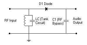
The Detector will be represented as follows: The LC tank assures that the input is effectively shorted to ground at DC and at audio frequencies as well as all RF frequencies except that to which it is tuned. The output is effectively shorted to ground at RF by C1.
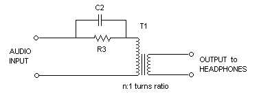
The Output Transformer circuit will be represented as shown below. The purpose of R3 and C2 will be covered later.
We start out with the assumption of no losses in the tuned circuits. This condition makes R2 equal to infinity, not a practical assumption of course, but it will simplify what follows. The input circuit then reduces to a simple series connection of the parallel tuned circuit, impedance transformed antenna voltage, and a series resistance. This resistance includes the effects of radiation, antenna, lead-in and ground circuit resistance. A simple transformation enables us to eliminate R2 entirely by combining its effects into a changed value for R1 and a new value for V1. The new value for V1 is: V1new = V1old*(R2old/(R1old + R2old)). The new value for R1 is: R1new = (R1old*R2old)/(R1old + R2old). With this transformation the new value for R2 is infinity, so it can be eliminated from the circuit. Of course, the maximum available power from the new source 'V1new, R1new' is less than what was available from the original source 'V1old, R1old' by the amount that was dissipated in R2. From now on, V1new and R1new will be referred to as V1 and R1. The RF Source Voltage (V1) is assumed to be un modulated CW. The transformed V1 (RMS) and R1 represent a Power Source of available power Pa = (V1^2)/(4*R1). This is the most power it can deliver to a load. It is also sometimes called the "Incident Power". For the load to absorb this power, the load itself must equal R1, and then it is called an 'Impedance Matched Load'. Changing the impedance transformation in the tuned circuit(s) changes the values of V1 and R1. This does not change the available power. That is still (V1^2)/(4*R1). As an illustration, if V1 is doubled, R1 must quadruple thus keeping the power the same. The approach we will use in this analysis is to minimize impedance mismatch power loss between the transformed antenna resistance and the diode detector input RF resistance as well as between the detector audio output resistance and the headphones. We will show that the diode detector power Loss (DDPL), for very weak signal levels, can be minimized by using a diode with as low a Saturation Current (Is) as possible if all else is equal. In addition, the lower the ideality factor (n) of the diode, the greater will be the sensitivity to weak signals. The limitation here is that if a diode with a lower Is used, the required diode RF source and audio load resistances go up in value. That limit is reached when the diode is connected to the top (the highest impedance point) of the tuned circuit. The high frequency audio cutoff point may be reduced because of unavoidable winding capacitance in the audio output transformer acting against the required higher transformed headphone effective impedance. The most important diode parameters to consider for Xtal set operation are saturation current 'Is' and 'n'. They show up in the Shockley diode equation: Id = Is*(exp((Vd-Id*Rs)/(0.026*n)) -1), at room temperature. In crystal radio set applications, the Id*Rs term may be neglected because it is usually much smaller than V. The equation then becomes: Id=Is*(exp(Vd/(0.026*n))-1). (1) This equation provides a good approximation of the V/I
relationship for most diodes, provided the parameters Is, n, and Rs are
really constant. Some diodes, especially germanium and silicon junction
diodes seem to have Is and n values which increase at very high currents
(higher than those usually encountered in crystal radio set operation).
In some of these diodes, the values of Is and n also increase at very
low currents, harming weak signal reception. Is and n are usually
constant in Silicon Schottky diodes, over the current range encountered
in crystal radio set use.
Agilent specifies the values of Is, Rs and n for Schottky diodes in their catalog. They are listed in the table of SPICE parameters. To find some SPICE parameters for other diodes (germanium types etc.), one can use used a neat Computer Program written by Ray Waugh of Agilent. To use it one measures the diode forward voltage at five different currents (0.1 mA, 1.0 mA, 4.8 mA, 5.0 mA and 5.2 mA). Ray&39;s program runs on Mathcad 6.0 or higher. One enters the five voltages and voila, out come Is, n, and Rs. Remember this caveat: The program assumes that Is, n and Rs are constant and do not vary with diode current. If they do vary, one can change the first two currents (0.1 and 1.0 mA) to cover a smaller range, say, two-to-one, that bracket a desired diode operating current and get the Is and n values for that current. Ray told me that if anyone wants a copy of this program, it would be OK for me to supply it. A simplified method of approximating Is (n must be estimated) that does not require having Mathcad is described in article #4. A complete description of a test set-up and calculation method for determining both n and Is is shown in Article #16. Here is what I have found experimentally through a SPICE simulation of a diode detector. If a detector diode is fed by an RF source resistance of n*0.026/Is ohms and is loaded by an audio load resistance of n*0.026/Is, then both input and output ports are matched with a return loss of better than 18 dB, assuming the signal is of weak to medium strength. This satisfies the condition of very low mismatch but only holds true for diode rectified currents of up to about 5*Is. An impedance matched diode detector insertion loss at a rectified current of 5*Is is about 3-4 dB. The input and output impedance match starts deteriorating with a DC rectified current of over about 5*Is because of the change from square law operation towards linear response at the higher input levels. At the highest RF Power input level point shown in the following graph, the rectified DC current is 500 nA and the input RF Return Loss (impedance match) is -12 dB. Diode detector power loss is 1.39 dB. At these high levels of Input Power, good matching conditions are restored if the Input Source Resistance is kept at n*0.026/Is and The Output Load Resistance is increased to 2*n*0.026/Is. If this is done input return loss goes to -26 dB and the insertion loss reduces to 0.93 dB. Here is a graph of Diode Detector insertion power loss of an Agilent 5082-2835 or HSMS-2820 Schottky diode detector driven by a 1.182 megohm source and loaded by a 1.182 megohm load. Note that these are very high resistance values for a usual Xtal set. The SPICE simulation was done using an Intusoft ICAP/4 simulator. Is of the diode=22 nA, n=1.03. The plot shows the insertion power loss as a function of the resultant rectified DC current. 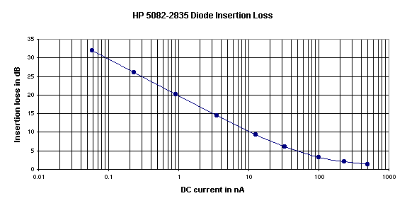
2.DISCUSSION In general, headphones should be impedance matched by a transformer to the output resistance of the diode detector. To use a diode of such a low Is as 22 nA with, say, a Brandes Superior 12k Ohm AC impedance 2k Ohm DC resistance headphones, an impedance transformation of 1,182,000/12,000 = 98.5:1 is needed (this high a ratio is hard to get). See Article #2, "Personalized Headphone Impedance" (PHI). One should be cautious of some small (maximum dimension of less than one inch) , high transformation ratio transformers because they may have a high insertion power loss. They also may also show the effects of nonlinear inductance because the initial permeability of the core is not high enough. Their shunt inductance is usually so low at low xtal set DX power levels, that the specified low frequency audio cut-off spec is not met. At the transformer's rated power level, the shunt inductance is generally high enough so that the low frequency cut-off spec is met. See Article #5 for info on various audio transformers. Headphones such as the 2000 DC ohm Brandes Superior
have an effective AC impedance of 12,000 ohms (PHI), but a DC resistance
of 2000 ohms. If the Brandes' impedance is incorrectly considered to be
12,000 ohms at DC and audio frequencies, and is used in a 12,000 ohm
circuit (without a transformer), too high a diode DC current will be
drawn because the DC resistance is really 2000 ohms, not 12,000. This
will load down the output RF tuned circuit thus reducing selectivity and
also give increased insertion power loss. For best selectivity
and minimum audio distortion at medium and high signal levels, the DC
load resistance on the diode should be the same as the AC audio load.
The solution to this problem is to place in series with the headphones a
parallel combination of a 10,000 ohm resistor shunted by a cap large
enough to bypass the lowest audio frequency of interest. When a
transformer is used; the parallel RC* (See R3 and C2 on the schematic
above.) should be connected in series with the low end of the high
impedance transformer primary winding. In this case the resistor should
equal the transformed effective headphone impedance (PHI). Another
advantage that accrues from adjusting the diode DC load to equal the AC
load has to do with the way selectivity varies as a function of
signal level. When the diode DC load is much smaller
than the AC load (the case when using a transformer and no
parallel RC), selectivity starts to reduce more and more
as signal strength increases above a moderate level. The reason is that
the detector rectified current increases very rapidly because of the
low DC diode load resistance. A high rectified DC current always
reduces the input and output resistances of a diode detector. Audio
distortion may also appear. Now make the DC load higher, say equal the
AC diode load impedance and have the detector impedance matched at both
input and output (at low signal levels). What happens then? As
the signal strength increases above a moderate level, the selectivity
will change by a much smaller amount because the RF resistance of the
diode detector will not drop as much as it did when the DC load
resistance was small. The resistance does not drop as much because the
DC rectified current is less because the DC diode load resistance has
been set to a higher value than before. Impedance matched conditions
also result in less power loss with consequently higher sound volume.
If the headphone effective impedance over the frequency range 0.3-3.3
kHz is transformed to a value lower than the output resistance of the
diode, these beneficial effects are reduced. If no transformer is used,
these effects may be hard to observe because the headphone effective
impedance will probably be lower than the output resistance of the
diode. Also, headphones usually have a resistive impedance component
about 1/6 the average value, and that goes part way towards being equal
to 80% of the effective impedance. What is the advantage of using a diode with a low Is? We will see that if matched input and output impedance conditions are maintained, diodes with lower Is give higher crystal radio set sensitivity (lower diode detector power loss) than diodes with higher Is, all else being equal. The statement above is especially important when dealing with low power signals that themselves result in high DDPL. The following graph shows the relationship between Diode Detector Power Loss at a relatively low DC Power Output Level (-66 dBm) vs. diode Is for diodes having an n of 1.03. Note that the graph data is valid only under the condition that the input and output are power matched.
NOTE: There is an error in the title of the graph. It should read: Detector Loss vs. Diode Is for a DC Power Output of -66 dBm. I used the -66 dBm signal level for the graph because it is related to the weakest voice signal I can hear with my most sensitive headphones, and still understand about 50% of the words. Here is the listening experiment that I used to determine that power level. I fed my headphones directly from a transistor radio through my FILVORA and reduced the volume until I judged I could understand about 50% of the words of a voice radio program. This enabled me to determine the average impedance of the headphones. (See article #2). I then measured the p-p audio voltage (Vpp_audio) on the headphones with an oscilloscope. Assume the AM station was running at about 100% modulation. The peak instantaneous audio voltage at the detector will be equal to Vpp_audio since the modulation is 100%. Now make the assumption that a CW carrier is driving the detector at such a level that the DC output voltage (Vdc) at the detector is equal to Vpp_audio. That DC voltage across a resistor of value equal to the detector load resistance will deliver an output power of Pdc=10*log((1000*(Vdc^2))/Rload) dBm. Since I could not get into the radio to measure the actual detector voltages and the audio load resistance, I used the p-p voltage measured across my 1200 Ohm headphones in place of Vdc to calculate the instantaneous power at the modulation peaks. Pp=10*log(1000*((Vpp_audio^2)/1200= -66 dBm. This power, Pp is that used in calculating the graph above. In my case Vpp_audio = 0.00055 Volts and effective headphone impedance = 1200 Ohms. To calculate the actual audio power level I was using in
the listening experiment, I assumed that the demodulated audio voltage
was a sine wave (not a voice) with the same p-p value as the actual
measured voice p-p voltage. It was then a simple matter to use the p-p
voltage of the assumed audio sine wave (Vpp_audio) and the effective
impedance (PHI) of the headphones to calculate the power of the audio
sine wave in dBm. P=10*log ((1000*(Vpp_audio^2))/(8*PHI)) dBm. This
value comes out 9 dB less than the DC power of -66 dBm. Of course there
is an error here in assuming that a sine wave of a specific p-p voltage
has the same RMS value as that of a broadcast voice waveform of an equal
p-p value. The "Audio Cyclopedia", in an article on VU meters, states
that the actual power from a voice signal is 8-10 dB less than the power
from a sine wave of the same p-p voltage. I'll use 9 dB. Bottom line:
The audio power from a voice voltage waveform is 18 dB less than the
audio power from a sine wave voltage of p-p value equal to the p-p
voltage of the voice waveform. We can now calculate that the electrical
power of weakest voice audio signal I can barely understand is -66 -9 -9
= -84 dBm. This figure depends on the sensitivity of the
headphones used and one's hearing acuity. I used a good sound powered
headphone set in this test. My hearing acuity is pretty poor. Keep in mind that diodes have an unavoidable back leakage resistance. Schottky diodes generally are very good in this respect. An exception is the so-called "zero bias" detector diodes. They have very high Is values and low reverse breakdown voltages and are generally not suitable for crystal radio sets. Germanium and cats whisker diodes are worse than Schottkys and vary greatly. This reverse resistance increases detector loss and reduces selectivity. "n" in the diode equation is usually close to 1.05 for Schottky barrier diodes. It is about 1.15 in Germanium diodes. All diodes have a fixed parasitic series resistance Rs. It is usually low enough to be ignored in crystal radio sets. One problem with Schottky diodes having a low reverse breakdown voltage and low Is is that they are more vulnerable to damage from static electricity than diodes with a higher leakage resistance. Tuned circuit loss and bandwidth considerations: A practical problem in using a diode of low Is is getting a high enough tuned circuit impedance for driving the diode. Of course, the first thing to do is to tap the diode all the way up on the output tuned circuit. An isolated tuned circuit having a typical Q of 350 at a frequency of 1.0 MHz, with a circuit capacitance of say 100 pF, and not coupled to an antenna or detector diode will have a resonant resistance of about 560k ohms. RF bandwidth will be fo/Q = 2.86 kHz. If an antenna resistance is now coupled in sufficiently to drop the resonant resistance by half to 280k, all of the available received RF power will be dissipated in the resonator, resulting in a bandwidth of 5.72 kHz (loaded Q of 175). If a diode is selected to match the now 280k ohm source resistance, it will present a 280k RF load resistance and result with a tuned circuit loaded Q of 87.5 giving an RF bandwidth of 11.4 kHz. The overall power loss caused by the tuned circuit loss is 3 dB. The diode will only receive 1/2 the maximum available-power at the antenna. The diode should have an Is of about n*0.026/278k = 100 nA (assuming a Schottky barrier diode is used). Note this: Even though the the diode is driven from a perfectly matched source (parallel connected combo of 560k tuned circuit loss and 560k antenna resistances), now the antenna does not see a matched load. It sees a parallel combo of the tuned circuit loss resistance of 560k and the 280k RF resistance of the diode. This is a resistance of 187k ohms. This mismatch power loss, included in the 3 dB above can be partially recovered by properly and equally mismatching the antenna and the diode. If this is done by more loss-less impedance transformation (technically, with an S parameter return loss of -11.7 dB), the total tuned-circuit power loss reduces to 2.63 dB, a reduction of 0.37 dB (pretty small, but it's there). If the ratio of unloaded to loaded tuned circuit Q was less than the 4:1 ratio used here, the loss reduction would be larger. Audio impedance transformation: One way to transform the 12k ohm effective impedance of a 2k ohm DC resistance Brandes Superior headset up to 280k ohms is to use an Antique Electronic Supply # P-T156, Stancor A53-C or similar 3:1 turns-ratio inter stage transformer. I measure an insertion power loss of only 0.5 dB with the following connection (See Articles #4 and #5 for other options.): 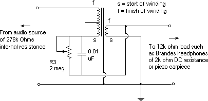 Note that the impedance transformation ratio is 16:1 thus stepping up the impedance of the 12,000 ohm headphones to 192,000 ohms not 278,000 ohms. This represents a mismatch of about 1.5:1. It will add a mismatch insertion power loss of only 0.15 dB. If the impedance mismatch had been 2:1, the insertion power loss would have been 0.5 dB. A 4:1 mismatch gives an insertion loss of 1.9 dB. The lead grounding the transformer lamination stack and frame is used if the transformer is mounted on an insulated material. It prevents the buildup of static charge on the frame during dry weather. Discharge of it might cause a crackling sound in the headphones or damage the diode (I got the crackling sound until I made the grounding connection). The transformer windings start and stop leads should be connected as shown to minimize the effect of the primary to secondary winding capacitance. If the f and s connections are reversed, the capacitance between the end of the secondary and the start of the primary winding will be across the primary and reduce the high frequency cut-off point. The lower impedance (secondary) winding is usually wound on the bobbin first, then after winding on several layers of insulation film, the higher impedance (primary) is wound. To determine how to connect the leads of the transformer, connect the primary and secondary windings as shown. (Disregarding the s and f notations). Connect an audio generator set to 1.0 kHz through a 200k ohm resistor. Load the secondary with a 12,000 Ohm resistor. Probe the input and output voltages with a scope. The output voltage should be about 0.25 of the input voltage. If the output voltage is about 0.5 that of the input, reverse the secondary leads. Repeat the test at 20,000 Hz and note the input and output voltages. Now reverse both the primary and secondary leads and repeat the 20 kHz test. The connection that gives the largest output voltage at 20 kHz is the correct one. Note that R3 is shown above as a rheostat not a fixed resistor. The nominal setting under the low signal level conditions discussed here is about 192k Ohms. Setting it to zero has little effect on reception of these low level signals. With this design approach, when receiving high level signals, RF selectivity is not reduced as much as when the DC resistance in the diode circuit is substantially below the effective impedance of the headset. When receiving very strong signals, R3 should be set for minimum distortion. One last comment: These design values are not critical. If impedances vary by several times from the optimum values, usually only a small sensitivity reduction will occur. What is the effect on the volume in the headphones of
a change of X dB? Many years ago I did a study which determined, in
a blinded condition, that a +1.0 dB or a -1.0 dB change in sound level
was barely discernible by most people. Half couldn't tell if the sound
level was changed or not after being told that a change might have
occurred. Another study had the listener listen to a sound. The sound
was then turned off for several seconds and then on again at the same
level, at a level of +3.0 dB or at a level of -3.0 dB. After the delay,
only half the listeners could tell whether the level of the sound had
changed or not. Incidentally, the listeners were not golden eared hi-fi
listeners. 4. SUMMARY
|
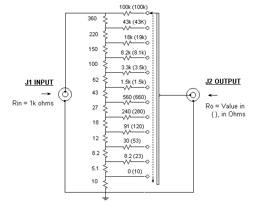
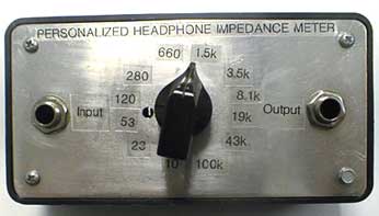
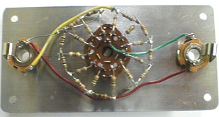
How to determine the effective impedance of magnetic headphones, a piezo-electric earpiece or a loudspeaker. No test equipment necessary
The magnitude of headphone or speaker impedance varies widely over the audio frequency range, being partly resistive and partly reactive. A 'Fixed Insertion Loss Variable Output Resistance Attenuator' (FILVORA) can be used to indicate the effective average value of this impedance, over that frequency range. The first section of this Article refers to the measurement of mono headphones and individual speakers by using a FILVORA. The second section describes how to use the FILVORA to determine the effective average impedance of each element in a stereo headset. The third section describes how the FILVORA was designed. |
|
 |
|
 |
 |
|
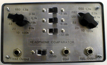
The circuit shown above has a fixed input resistance of 1000 ohms +/- about 5%, no matter what load is connected the output or where the switch is set. The output resistance at any switch point is about +/- 5% of the value shown with any impedance driving the input. The insertion loss of the FILVORA is 26 dB. Standard 5% tolerance resistors are used. The use of resistors that differ by +/- 10% from the values shown should not have an appreciable impact on performance of this unit. To use the FILVORA, connect a source of audio voice or music to the input jack J1. (I use the output jack of a transistor radio for my source.) Connect the plug of the mono headphone set or speaker to be measured to the output jack J2 of the FILVORA. Adjust the switch for the loudest volume. The correct setting indicates the effective impedance is very broad and somewhat hard to determine. Call it P2. Rotate the switch in one direction from P2 for a small reduction in volume to position P1 (generally a two positions movement), then in the other direction from P2 by two positions to P3. If the volume at P1 and P3 are the same, P2 indicates the effective impedance of the headset. If the volume at P1 and P3 is not the same, increment both the P1 and P3 settings ccw or cc by one position. When you obtain the same volume at the new P1 and P3 positions, you are done. The effective headphone impedance is the calibration indication of the switch at point P2. Sometimes equal volume settings cannot be obtained with switch settings five positions apart. If this is the case, try to get equal volume settings four positions apart. If this is done, the effective impedance is equal to the geometric mean of the settings of P1 and P3. (Take the square root of the product of the calibration readings at P1 and P3.) The effect of source impedance on tone quality. It is interesting to note, that with magnetic elements, setting the switch to a high source resistance tends to improve the treble and reduce the bass response, compared to the response where the source matches the effective impedance of the element. Setting the switch to a low resistance does the reverse. This setting rolls off the treble, and relatively speaking, improves the bass. With piezo ceramic or crystal elements, a high source resistance tends to reduce the treble and improve the bass response, compared to the response where the source matches the effective impedance of the element. A low source resistance tends to reduce the bass and emphasize the treble. Some piezo elements sound scratchy. This condition can be minimized by driving the elements from a lower average impedance source. Here are some practical experimental ways to vary the audio source resistance of a crystal radio set when receiving medium strength to weak signals. A medium strength signal is defined as one at the crossover point between linear to square law operation (LSLCP). See the graphs in Article #15A.
If you are interested in DX reception with headphones and do not have normal hearing, you might want to customize the source resistance driving the headphones. This enables using the 'change in headphone frequency response as a function of headphone driving resistance' to partially compensate for high frequency hearing loss. Input a voice signal and reduce its volume to a sufficiently low level such that you judge you understand about 50% of the words. Readjust the switch to see if you can obtain greater intelligibility at another setting. If you can, this new switch setting indicates the source resistance with which to drive the particular headphones being used to deliver maximum voice intelligibility for your ears. I call this resistance: Personalized Headphone Impedance (PHI). For magnetic headphones, this resistance is higher than the average impedance of the earphones, for piezo-electric ceramic earpieces, the resistance is lower. Two FILVORA units enable one to compare
the actual power sensitivity of two headphones, even if the effective
impedance the two headphones are very different. A dual unit to do this
(DFILVORA) is described in Article #3. The effective impedance of hi-fi stereo headphones may
be checked with the FILVORA. The effective impedance of the two
earpiece elements can be checked by determining the switch position for
maximum volume with one of these connections: (1) The sleeve, to the
ring and tip in parallel or (2) the ring to the tip. Measurement (1)
will show one half the effective impedance of one earpiece and
measurement (2) will give a reading of two times the effective impedance
of one element. To help define the equations used to calculate the the resistor values for the asymmetrical attenuator 'FILVORA' the following requirements were set up:
A system of 25 simultaneous was written and solved in MathCad for the values of the 24 resistors. Those are the values (5% resistor series) shown in the schematic. To minimize power loss, the attenuator becomes an inverted L minimum-loss pad at the two extreme switch positions. It is a non-minimum loss T pad at the intermediate positions. The output resistance range of the FILVORA is 10,000 to 1. This establishes the minimum loss. If the output resistance range were 100,000 to 1, the insertion loss would have to be 31 dB. Insertion power loss = 5*log(resistance ratio)+6dB. |
|
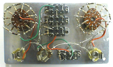
Compare the impedance and sensitivity of headphones, earphones and/or speakers even if they differ greatly in impedance. No test equipment necessary
|
The purpose of this article is to show
how to compare the sensitivity of two pair of speakers or mono
headphones even if they differ greatly in effective impedance.
See Article #2 on how to measure impedance. The Dual Fixed
Insertion Loss Variable Output Resistance Attenuator (DFILVORA)
will be described and directions for its use will be given in
Section 1. It is essentially a combination of two FILVORA units
along with some extra attenuators. Section 2 will describe how
to modify the DFILVORA for use with Hi-Fi stereo headphones.
Note: The use of resistors that difer by +/- 10% from the
values shown in the schematic should not have an appreciable
impact on performance of this unit.
|
 |
 |
|
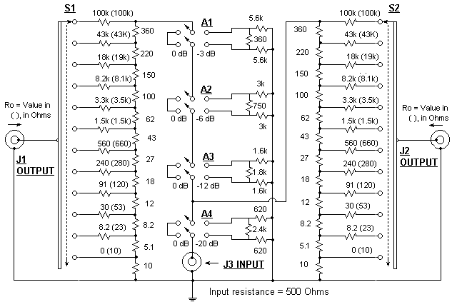
Connect an audio source to jack J3. (I use the output jack of a
transistor radio for my source.) Connect the plug of one of the
two mono headphone sets or speakers to jack J1 and the other to
jack J2. Set attenuators A1, A2, A3, and A4 to 0 dB. Switch S1
should be set to the position providing the loudest sound in the
headphone set or speaker connected to J1. Switch S2 should be
set to the position providing the loudest sound in the unit
connected to J2. (Read Article #2 to see the recommended
procedure for doing this.) If the unit connected to J2 is
louder than the unit connected to J1, reverse the units. Now
add attenuation in the path to the unit connected to J1 in 3 dB
steps by using A1, A2 and A3 in the proper combinations (the
dB's add), until the volume from the unit connected to J1 equals
the volume in the unit connected to J2 as closely as possible.
If the sound cannot be reduced to a low enough level because of
volume control limitations in the INPUT source, use A4 to reduce
the volume by 20 dB.
The sum of the dB settings of A1, A2 and A3 equals
the difference in power sensitivity between the two
headphones or speakers, independent of the effective impedance
of the units. The settings of S1 and S2 indicate the average
impedance of the two units. See Article #2 for more details on this
subject. The power insertion loss from jack J3 to either jack J1 or
jack J2, with the attenuators set to zero, is 29dB. To compare the power sensitivity of two stereo headphones, I recommend that several modifications be made to the DIFLVORA. Jack J1 should be changed to a stereo jack and the ring and tip connections tied together. The same change should be made to J2. this will cause each stereo headphone to be tested in mono mode with its elements connected in parallel. The value of all resistors should be halved. The setting of switches S1 and S2 indicate the average impedance over the audio frequency range of two earphone elements in parallel, and that figure will be one-half the value of each element by itself. Also, the measurable range of individual element impedances will be changed from 10 to 100k Ohms to 20 to 200k. The range of impedance measurable for the parallel combo of two elements is still 10 to 100k Ohms. To correct this condition and have the DFILVORA switches S1 and S2 indicate the value of the impedance of one element (and not two in parallel), halve the value of all resistors in the schematic. If this modified DFILVORA is now used to measure a mono headset, the resistance readings of switches S1 and S2 will be twice the actual value. These modifications change the input resistance of the DLVORA to 250 Ohms. |
|
The best diode and audio transformer for a crystal set, and a way to measure diode saturation current Here is a practical way to determine the diode and audio output transformer impedance matching characteristics needed to maximize sensitivity and selectivity for weak signals and to reduce strong-signal audio distortion in a Crystal Radio Set. Unfortunately, this may be an iterative process.
What we have done here is to minimize loading on the tuned circuit from the diode detector. If this diode loading is made negligible, using a resistor of value equal to that of the resonant resistance of the tuned circuit will reduce the RF voltage to 0.5 of what it was before the resistor was placed. Here, the diode has been given a high resistance DC load to further reduce its loading effect on the tuned circuit (the 10 Meg resistor connected in place of the headset). The detector is used as an indicator of the RF voltage across the tank circuit. The diode will be operating somewhere between linear and square law. That is where the 0.35 comes from (geometric mean of 0.5 and 0.25). A Better approach, if one has a high sensitivity scope good to above 1.0 MHz, is to disconnect the diode from the tuned circuit. Then very lightly capacitively couple the scope to the tuned circuit and use it as a measuring tool when placing the resistor across the tuned circuit. Then of course, one would use the 0.5 figure for voltage reduction since the measurement is linear. Bear with the problem of the measured voltages jiggling up and down due to modulation. Just estimate an average. (See Article #0 for information on diode Saturation Current and Ideality Factor.) #2. A good diode to use in the crystal radio set above, for weak signal reception, is one with an axis-crossing resistance equal to Rr. A diode that has an axis-crossing resistance of Rr is one having a Saturation Current of Is = (25,700,000*n)/Rr nanoAmps. The ideality factor of the diode (n) is an important parameter in determining very weak signal sensitivity. If all other diode parameters are kept the same, the weak signal input and output resistances of a diode detector are directly proportional to the value of n. Assume a diode with a value of n equal to oldn is replaced with an identical diode, except that it has an n of newn; and the input and output impedances are re-matched. The result will be a detector insertion loss change of: 10*log(oldn/newn) dB. That is, a doubling of n will result in a 3 dB drop in power output, assuming the input power is kept the same and impedances are re-matched. This illustration shows the importance of a low value for n. Back leakage resistance should be low and the diode series resistance (Rs) should also be fairly low. Diode barrier capacitance should be fairly low (6 pF or less) . Schottky barrier diodes usually have low series resistance, barrier capacitance, Ideality Factor and very low back leakage. The challenge is to get a diode reasonably close to the correct Is. (If it's within 0.3 and 3 times the calculated value, you won't notice much difference.) A simple way to check for back-leakage is to measure the back resistance of the diode with a non-electronic VOM such as the Triplett 630 or Weston 980. Use the 1000X resistance switch position. If no deflection of the meter can be seen, the diode back leakage is probably OK. Another way is to place a DC blocking capacitor in series with the diode. If the audio becomes very distorted, the diode leakage is low (this is the desired result). A value of 1000 pF or so is OK for this test. Here is an easy way to determine the approximate Is of a diode. Forward bias the diode at about 1.0 uA. A series combination of a 1.5 volt battery and a 1.5 Meg resistor, connected across the diode will do this. Measure the voltage developed across the diode with a DVM having a 10 Meg input resistance. Calculate Is=667*(Vb-Vd)/(e^(Vd/(0.0257*n))-1) nA. e = base of the natural logarithms = approx. 2.718, ^ = "raise the preceding number to the power of the following number", Vb = voltage of the battery, Vd = voltage across diode and n = diode Ideality Factor (Emission Coefficient). I suggest using an estimate of 1.12 for n. Most good detector diodes seem to have a n between 1.05 and 1.2 A method for measuring both n and Is is shown in Article #16. Measurements on 1N34A germanium diodes at various currents show that the values for Is and n are not really constant, but vary as a function of diode current. Is can increase up to five times its value at low currents when currents as high as 400 times Is are applied. However, germanium diodes I have tested exhibit a fairly constant n and Is when measured at currents below about six times their Is. A rectified current of about 6 times Is corresponds to a fairly weak signal. The following chart shows some results from measuring several diodes at a current of 1.0 uA. The calculated low-signal-level value of the diode junction resistance Rj= 0.0257*n/Is is is also given. Note the wide variation among the various diodes sold as 1N34A. Schottky diodes, as a rule are fairly consistent from unit-to-unit. The Agilent '2835 measured 11 nA, and many others test close to this value. I think that many years ago early production '2835 diodes probably matched the Spec. sheet value of 22 nA for Is. Over the years, I would guess that the average value was allowed to drift in order to optimize other more important parameters (for most applications) such as reverse breakdown voltage. BTW, Is is not a guaranteed 100% tested production spec. Caution: If one uses a DVM to measure the forward voltage of a diode operating at a low current, a problem may occur. If the internal resistance of the DC source supplying the current is too high, a version of the sampling voltage waveform used in the DVM may appear at its terminals and be rectified by the diode, thus causing a false reading. One can easily check for this condition by reducing the DC source voltage to zero, leaving only the diode in parallel with the internal resistance of the source connected to the terminals of the DVM. If the DVM reads more than a tenth or so of a millivolt, the problem may be said to exist. It can usually be corrected by bypassing the diode with a ceramic capacitor of between 1 and 5 nF. Connect the capacitor across the diode with very short leads, or this fix may not work. If one wishes to screen a group of diodes to find one having a specific Is, use the setup described above. Substitute the desired value of Is into the following equation: Vd=0.0282*ln(667*(Vb-Vd)/Is+1) volts. 'ln' means natural base logarithm and Is is in nA. A diode having a Vd equal to the calculated value will have approximately the desired Is. Here are some tips to consider when measuring diodes: Keep all leads short and away from 60 Hz power wires to minimize AC and electrostatic DC pickup. Place a grounded aluminum sheet on the workbench, and under the DVM and other components to further reduce spurious pickup by the wiring. A piece of grounded kitchen aluminum foil will do nicely for the aluminum sheet. You may find that the reading of Vd slowly drifts upwards. Wait it out. What you are observing is the temperature sensitivity of Vd to heat picked up from handling the diode with your fingers. Let the diode return to room temperature before taking data. Many glass diodes exhibit a photoelectric effect
that can cause measurement error. Guard against it by checking to
see if a diode current reading changes when the light falling on the
diode is changed.
Note that these values for Is and n are not cast in stone. Is can easily vary by 2:1 or more from diode to diode of the same type. Multiple similar diodes may be paralleled to increase Is. Is is increased proportionally to the number of diodes in parallel. Four identical diodes in parallel will give a saturation current four times the Is of one alone. For purposes of Crystal Set design, diodes should not be placed in series. SPICE simulation shows that if two identical diodes are connected in series, the combination will perform the same as one of the diodes alone, but having a doubled value for n. This increased value of n will reduce weak signal sensitivity. In a particular crystal radio set Is can vary quite a bit without a great effect on performance. One can be in error by several times and still get good results. Too high an Is reduces selectivity on weak signals. Too low a value reduces sensitivity to weak signals and causes excessive audio distortion. Many times the question is asked, "What is the best diode to use?" The answer depends on the specific RF source resistance and audio load impedance of the Crystal Set in question. At low signal levels the RF input resistance and audio output resistance of a detector diode are equal to 25,700,000*n/Is Ohms (current in nA). For minimum detector power loss at very low signal levels with a particular diode, all one has to do is impedance match the RF source resistance to the diode and impedance match the diodes' audio output resistance to the headphones by using an appropriate audio transformer. The lower the Is of the diode, the higher will be the weak signal sensitivity (volume) from the Crystal Set, provided it is properly impedance matched to it's circuit (see article #1). This does not affect strong signal volume. There is one caveat to this, however. It is assumed that the RF tuned circuits and audio transformer losses don't change. This can be hard to accomplish. It is assumed that the Rs, diode junction capacitance, n and reverse leakage are reasonable. If the diode you want to use has a higher Is than the optimum value, tap it down on the tuned circuit. If the diode you want to use has a lower Is than the optimum value, change the tank circuit to one with a higher L and lower C so that the antenna impedance can be transformed to a higher value and repeat step #1. If you don't have a diode of the proper
calculated Is, you can simulate what the result would be if you
did have one by doing the following: Put a small voltage in series
with the DC load resistor ground return (see point #4 below). If
your diode has too low an Is, biasing the diode in the forward
direction will improve sensitivity. If your diode has too high an
Is, biasing the diode in the reverse direction will improve
sensitivity. See Article #9 on the home page on how to build and
use a "Diode Detector Bias Box". #4. The average audio impedance of the headphones should be transformed up to the value Rr by an appropriate audio transformer. The step-down impedance transformation ratio needed in the transformer is Rr/Zh. When connecting the transformer high impedance winding to the diode, put a parallel RC (a benny) in series with the ground connection . This will insure that the DC load on the diode can be made the same as the audio AC load. A good value for the R should be about equal to Rr. It's best to use a pot so that the value can be optimized at different signal levels. For minimum audio distortion at medium and high signal levels, the DC load on the diode should be the same as the AC audio load. The value of the C should be large enough to fully bypass the R for audio. A good value is C=5/(pi*2*300*Rr). The parallel RC will have less effect on reducing distortion or affecting selectivity when receiving loud signals if the transformed headphone load on the diode is lower than the diode output resistance, than if it is higher. For info on the impedance transformation ratios of various transformers see Article #5. The audio transformer should have a low insertion loss. Try to obtain one with less than 2 dB loss from 300-3300 Hz when measured at low Crystal Set signal levels. See Article #5 for info on how to measure transformer Insertion Loss. #5. Connect up the new diode and transformer and the parallel RC. Trim up the value of the R in the parallel RC for the least audio distortion on a loud signal. There should be an improvement in low signal volume and high signal audio distortion as well as better selectivity. |
|
Impedance matching for magnetic and
piezo-electric headphones, measurements on several audio transformers,
and a transformer loss measurement method Quick Summary: This Article discusses the use of audio transformers with crystal radio sets and gives the results of loss measurements on several of them. A method for measuring insertion power loss is also described. Many crystal radio set designs provide impedance step down taps on the final RF tuned circuit. If the diode is connected to one of these taps, its loading on the tuned circuit is reduced and selectivity is improved. Too much of a step down also reduces sensitivity. RF tuned circuit loading by the diode is affected by the diodes' Saturation Current, the headphone effective impedance and the signal level. One can reduce the loading effect of headphone effective impedance and of high signal level by transforming the headphone impedance up to a value that matches the audio output resistance of the diode detector itself. This approach can keep the selectivity high and also increase the sensitivity of the crystal radio set. For info on measuring headphone effective impedance see article # 2. It is important that the diode sees a DC load equal to its AC audio load. This will permit connecting the diode to a higher tap or maybe to the top of the tuned circuit. The result will be to maintain selectivity and reduce audio distortion for medium and especially for strong signals. Diodes of lower Saturation Current can be tapped up higher on the tuned circuit than those of higher Saturation Current and, all else being equal, will give higher receiver sensitivity. See articles #0, #1, #4 and #15. 1. Setup for switchable Transformation Ratios using the A.E.S. P-T157 or an equivalent Transformer. The sensitivity improvement mentioned above will only be attained if the audio transformation is performed with a low insertion loss audio transformer. For experimental purposes one of the best transformers I have found is the P-T157 from Antique Electronic Supply. What immediately follows is the description of two switchable circuits that can supply various transformation ratios for driving a 12k Ohm load. This is the nominal AC impedance of most 2,000 DC Ohm headphones, as well as many piezo electric ceramic earpieces. Later on, specific non-switched configurations are shown for several different transformers. Since this Article was written, A.E.S. has stopped selling the P-T157. Results close to those shown below can be obtained using the A.E.S. P-T156, Stancor A-53 or most any 3:1 turns ratio tube-type inter-stage audio coupling transformer. A good description of this type of transformer is: A transformer designed for plate-to-grid inter-stage coupling, having a 3:1 turns ratio, and specified for a 90k to 10k ohm impedance transformation. Henceforth, in this Article, this type of transformer will be referred to as a "3:1 AIT". Note that the switched transformation ratios shown below
vary by a factor of about four from one to another. Note also that an
impedance mismatch of 2:1 gives an insertion loss of only 0.5 dB. This
means that all values of diode output resistance from 12k Ohms up to
750k can be utilized, with a mismatch insertion loss of no more than a
maximum value of 0.5 dB, plus the transformer loss. Measured
transformer loss is about 1.0 +/- 0.5 dB from 300- 3300 Hz at the 63
times ratio and about 0.5 +/- 0.2 dB at the 16 and 4 ratios. Note: The
transformation ratio on the H switch position is shown as 63 instead of
72 because of shunt resistive losses in the transformers. On this
switch position the diode sees the 12k headphones transformed to 750k,
not 860k. T1 and T2 are preferably Antique Electronic Supply P-T157
transformers. Alternatively, one can use most any generic "3:1 AIT".
One will get a small amount more loss with the alternatives, mainly at
300 Hz and when the signal is weak. C2 can be used to peak up response
at 300 Hz if a generic "3:1 AIT" transformer is used. C2 can be omitted
if the P-T157 transformers are used. Experiment with values around 0.02
uF. Sw1 and Sw2 are DPDT slide or toggle switches. R can be a 1 Meg
pot. It is used to set the diode DC load resistance to be equal the
transformed AC load impedance.* A log taper is preferred. Set R for
the lowest audio distortion and best selectivity on strong signals. The
diode load at DC must be the same as for AC audio signals for best
results. This setting has little effect with weak signals, however. C1
should be about 0.05 uF. See the later part of Article #1 for info on
determining transformer winding polarity and how to reduce the effect of
inter-winding capacitance.
Fig. 1 There is no need to transform headphone effective impedance up to as high as 750k unless the RF tuned circuit, when loaded with the antenna, has a resonant resistance of around 750k Ohms. It is very difficult to attain an impedance this high. The diode also would have to have the appropriate Saturation Current of about 38 nA. For experimental purposes, if a transformed impedance of no higher than 380k is desired, a one transformer circuit should be used as shown below. This will prove more practical in real world applications. R may be a 250k or 500k Ohm pot, preferably with a log taper. The transformer insertion loss remains below 1.0 dB from 0.3-3.3 kHz with output loads between from 6k to 24k Ohms when using the A.E.S. P-T157. Keep in mind that the saturation Current (Is) of the diode should be such that the diode's (Weak signal) RF input resistance is about equal to the (Antenna loaded) RF tuned circuit resonant resistance and also to the transformed headphone effective impedance. This diode resistance is equal to (0.0257*n)/Is. Is is in Amps. For more information on this, see article #4 listed on the home page.
2. Practical Fixed Transformation Ratio
Setups using the A.E.S. P-T157, PT-156, Stancor A-53
or similar The following schematics show various connections for the transformers mentioned above. The connections are arranged to provide various diode audio frequency load impedances from headphone loads of either 12,000 or 1,200 Ohms AC impedance. The 12,000 Ohm connection is appropriate for most magnetic headphones of 2,000 Ohms DC resistance and many piezo earpieces. The 1,200 Ohm connection is used when driving a series connected set of typical sound powered elements. As stated before, it is important that the diode have a DC load of the same value as its average AC load. This can easily be accomplished by placing the parallel combination of a pot with an audio bypass capacitor in series with the lead marked 'RC' between the points marked "x--x" (see below). The pot should have an audio taper and be connected as a rheostat. 0.5 to 1 Meg is usually a good value. The value of the capacitor depends upon the impedance reflected into the transformer primary from the headphones. A value of 0.05 uF or more is usually OK. The pot should be adjusted to minimize distortion and improve selectivity when receiving strong signals. Its setting has no effect when receiving weak signals.
First, some help. In schematics A-F it is important to properly phase the windings. For best performance at the high end of the audio band, one should minimize the effect of transformer inter-winding capacitance. This is most important to do when using circuits D or E, but has little effect when using circuits A, B, C, or F. To do this, the start and finish leads of the transformer coils must be properly connected. In the schematics shown above, the start and finish of the transformer windings are indicated by "s" and "f". The start of the low impedance winding of a PT-156 or P-T157 transformer is the blue lead. The finish is the red lead. The green lead next to the red lead is the start of the center tapped high impedance winding. The green lead next to the blue lead is the finish. If Stancor A53-C transformers are (is) being used, the color coding is different. The start of the low impedance winding is the red lead, the finish is the blue lead. The green lead of the center tapped winding next to the blue lead is the start, and the green lead next to the red lead is the finish. The insertion loss values shown below are were measured
using A.E.S. P-T157 transformers. Stancor A53-C or generic "3:1 AIT"
units will perform somewhat worse, as mentioned above. If you are going
to use a generic "3:1 AIT", keep in mind that all or most of the
extra insertion loss at 0.3 kHz can be eliminated by using the correct
capacitor in series between the transformer and headphones.
A very low loss transformer that can be used to transform a 1 Megohm source down to closely impedance match a 12k AC ohm load is the small UTC O-15 'Ouncer' transformer. Its insertion power loss is less than 1 dB from 0.3-3.3 kHz.
Here are general specifications for the A.E.S. P-T157, Stancor A-53C and generic "3:1 AIT" Inter-stage transformers: Single Plate (10,000 Ohms) to push-pull grids (90,000 Ohms). Overall turns ratio: 1 to 3 Primary to Secondary. Max. Primary DC: 10 mA. These transformers are still relatively cheap and usually available at Hamfests, personal junk boxes and Used Component Vendors. 3. Transformer configurations for use mainly with Sound Powered Headphones. Now we will talk about some other transformer configurations that are suited for use with Sound Powered phones: UTC LS-10, UTC A-10, UTC A-12, Amertran 923A and UTC C-2080, as well as many others. The UTC A-10 and A-12 have the same terminal impedance specifications as the LS-10 and will probably perform similarly. Some of these transformers are currently quite expensive. For some lower cost options, see Part 5 of this article for some generic transformer specs., or consider the last two connections shown in the chart above. Shown below are loss measurements using a physically very small, but very low cost transformer, the MOUSER TM-117 as well as two excellent small low loss transformers from the CALRAD line. At the end of this Section (#3), measurements on a combination of two transformers are be shown that enable 900k to 1200 ohm and 470k to 1200 ohm impedance transformation. Six measurements on the TM-117 are shown. The first
test of the transformer is with the input and output resistance values
specified by the Manufacturer, but at a low output signal level. The
second is for a TM-117 driven and loaded by resistances (24k ohms
primary and 300 ohms secondary instead of 50k ohms primary and 1k ohms
secondary). The 24k ohm level is close to that delivered by a generic
1N34A diode when detecting a weak signal. The next three measurements
are for four TM-117 transformers interconnected to give a transformation
ratio four times greater than one gets from one transformer alone. The
primaries are connected in series and the secondaries are connected in
series/parallel. The resultant primary and secondary are connected as
an autotransformer. Results are given from measurements made at three
output power levels. The last measurement is with the transformers
connected for a 1,200 Ohm output instead for a 300 Ohm output. Most
Sound Powered elements I have seen have an AC impedance of about 600
Ohms when averaged over the frequency range of 0.3-3.3 kHz. When used
as a 1,200 Ohm transformer load, the two elements should be connected in
series. When used as a 300 Ohm load, the elements should be connected in
parallel. Remember that the insertion loss near 0.3 kHz can usually be
reduced by placing a proper capacitor in series with the connection from
the transformer to the sound powered headphones.
* The UTC-2080 is rated by the manufacturer for transforming
between source/loads of 100 and 100k Ohms. A similar
transformer made by the Stanley Company (TF-1A-10-YY) is (or
was) offered by the Fair Radio Sales Co. as #T3/AM20, for about
$7.95. They are recommended as good all around choices for
driving 300 ohm sound-powered phones (SP elements in parallel)
in good quality crystal radio sets.
To obtain the approximate magnetizing inductance, resonant
resistance and distributed capacitance for the UTC and Stanley
units that appears at terminals 3 and 4 (other winding
open-circuited), multiply the values of the first two parameters
above by 1000 and divide the distributed capacitance by 1000.
This is because of the 1:1000 impedance transformation ratio.
Note: Terminals 1 and 2 are marked as the "100" ohm terminals, 3
and 4 are marked "100k". Bear in mind that the magnetizing
inductance of these transformers can vary appreciably from
sample to sample because of the low (or no) air-gap design used
in the laminations.
*Some or all of the loss at 0.3 kHz can be eliminated by
coupling the transformer to the headphone load through a series
capacitor. This makes a high pass filter with a cutoff
frequency at or somewhat below 0.3 kHz out of the components,
instead of having a just a plain old shunt parallel RL 6
dB/octave roll-off response. The components of the filter are
the shunt inductance of the transformer, the series capacitor
and the shunt inductance of the headphone impedance. A value
around 2 uF is usually good if the headphone effective impedance
is 300 Ohms (elements connected in parallel). A value around
0.5 uF is good if the headphone effective impedance is 1,200
Ohms. (Elements connected in series) One must experiment with
different values because the inductance and effective impedance
of different elements varies from Mfg. to Mfg. Of course, this
principle may be employed at other impedance levels such as the
12k ohms in a Brandes Superior headset, when used with an
appropriate transformer (see the paragraph above Fig. 1).
The transformer loss figures for the UTC and AMERTRAN transformers were measured at an output power of about -60 dBm. Performance is retained at output power levels much less than -60 dBm. A voice signal at this power level will be quite soft, but understandable through most sound powered headphones. The MOUSER transformer deserves special discussion since it is so low in cost. Frequency response and distortion: The loss figures at two different power levels for a TM117 purchased in March of '00 are as follows: Output power level of +15 dBm: 2.8 dB @ 0.3 kHz, 1.9 dB @ 1.0 kHz and 6.4 dB @ 3.3 kHz. Output power level of -60 dBm: 11.1 dB @ 0.3 kHz, 1.8 dB @ 1.0 kHz, 5.7 dB @ 3.3 kHz and 5.4 dB @ 0.6 kHz. The 0.3 kHz loss is greater at a power level of -60 dBm than at +15 dBm. Why? The core laminations of the TM-117 (and many other very small transformers) have low permeability at the low magnetic flux levels generated by the -60 dBm signal. This low permeability is called initial permeability. The initial permeability, in combination with other factors, results in the transformer having a specific shunt inductance (at low signal levels). This shunt inductance controls the low frequency roll-off of the transformer. At higher flux levels (signal levels), but before saturation occurs, the permeability increases to an "effective permeability" value which can be several times greater than the initial permeability. This means that the transformer shunt inductance is higher at the higher signal level and the low frequency roll-off is much reduced. There may be some production unit-to-unit variation in the low frequency response of the TM117. One that I bought about a year ago showed 2.5 dB less loss at 0.3 kHz than the one tested above. Some low frequency harmonic distortion is generated in the changeover region from initial to effective permeability. This can easily be seen on a 'scope, especially at 300 Hz sine wave. I doubt that it would be very noticeable in actual crystal radio set use. One can see from lines three, four and five of data in the TM-117 Insertion Loss Chart above, that the loss at 0.3 kHz, relative to that at 1.0 kHz, gets less as the output power level is increased. The loss at 1.0 kHz is minimum at the -42 dBm output power level. The greater 1.0 kHz loss at the -72 dBm power level is caused by the reduced shunt inductance as explained above. The increase in 1.0 kHz loss at -42 dBm occurs because the core is getting closer to saturation. The loss at 3.3 kHz in the four-transformer configuration is greater than that for one transformer shown on line 2 because the primary-to-secondary capacitance of transformers A and B is effectively connected from high impedance points and ground, thus rolling off the high end response. The single transformer in line 2 is wired so that the primary-to-secondary capacitance is not in shunt across the primary to ground. The CALRAD line of small transformers offers two
types that are suitable for use in transforming a high diode detector
output resistance down to 300 or 1200 Ohms to drive SP phones. Their
insertion loss is quite low and within a fraction of a dB of that of
the UTC LS-10. One distributor of CALRAD transformers is Ocean State
Electronics, 6 Industrial Drive, P.O. Box 1458, Westerly, RI. The two
transformers are #45-700, spec'd to transform 100k to 1000 Ohms and
#45-703, spec'd to transform 200k to 1000 Ohms. They sell for $5.95
ea. The following chart shows the measured performance of a single
transformer and of combinations of two. Lines #1 and 2: Primaries are
in series, secondaries in parallel. Line #3: Primaries are in
parallel, secondaries in series. Performance is very good, especially
so, considering the price.
* See asterisk just below the preceding Mouser
transformer table.
Note: The hot lead of the high impedance winding should always be the red lead. The hot lead of the low impedance winding should be the white lead. The high impedance windings are connected in series in lines 1, 2, 6 and 7. They are in parallel in line 3. The low impedance windings are connected in parallel in lines 1, 2, 6 and 7 with leads of like color connected together. The hot low impedance output connection is to the white leads. The other two joined leads go to ground. The low impedance windings are connected in series in line 3. One must properly phase the windings when two transformers are used. The lead from the hot end of the high impedance winding of transformer #1 should be connected to the diode. Its cold lead should go to the hot lead on transformer #2. The cold lead of transformer #2 should go to a parallel RC, the other end of which should either go to ground in lines 1, 2, 3, and 7 or to the hot low impedance output in line 6 (autotransformer connection). In line 7, transformer #1 should be the 45-703.
The R1 C1 combination is sometimes called a "benny". It is used to reduce audio distortion sometimes encountered on strong stations. A good value for the pot, R1, is 1-3 Megs, preferable with an audio taper. C1 is not critical. A value of 0.1 uF is suggested. A typical diode for use with this transformer assembly is a one having a saturation current of about 22 nA, such as the Agilent 5082-2835 or HSMS-2820. The weak signal audio output resistance of such a diode, as well as the input audio resistance of this transformer assembly shown in Fig. 4a are each about 1.35 Megs, making their parallel combination about 675k ohms. If the total shunt capacitance at this point is about 70 pF, audio frequencies above 3.3kHz will be attenuated by more than 3 dB. This capacitance consists of the sum of the windings capacitance of the transformer assembly referred to its input, wiring capacity to the diode and the junction capacity of the diode, etc, all in parallel with the RF bypass capacitor of the detector (C9 in Fig. 5 in Article #26). When using this transformer assembly, if the audio high frequencies seem deficient, try reducing that capacitor (C9), or maybe eliminating it and depending upon the other capacitive elements for RF bypassing. If one possesses good high frequency hearing, a higher impedance tap than normal may strengthen the highs. This is because the impedance of magnetic headphones is not constant. It rises as frequency increases, therefore, a better impedance match will exist for high frequencies when a higher impedance tap than normal is used. See "The effect of source impedance on tone quality" in Article #2.
4. How to Measure the approximate Insertion Power Loss of any Audio Transformer, or Compare its Performance to that of an Ideal no-loss Transformer The equipment needed are an audio sine wave generator, an assortment of resistors (preferably not a resistance box), and a high sensitivity scope or DVM. The use of a vertically calibrated scope is preferable to a DVM, as one can see that the waveform is clean and without appreciable hum or noise. A difficulty with this approach is that one must make sure that the scope decade attenuator as well as the 10X switch on the probe are accurate. I use the scope probe switched to 1X when reading the low voltage secondary voltage and to 10X setting when measuring at the higher voltage primary. The high input impedance of the probe prevents excessive loading of the high impedance primary, thus reducing the voltage there and causing an incorrect reading. Connect the hot lead of the generator to the high impedance primary of the transformer through a resistor of value equal to Rs. Rs should be equal to the expected output resistance of the diode detector. Connect a load resistor Rl of value Zh (expected effective impedance of the headphones) to the secondary. Connect all grounds to a common point. Tune the generator to the first frequency of measurement, say 1000 Hz. Connect the scope or DVM to the low impedance secondary. Adjust the audio generator to as low a level as possible while still being able to get an accurate reading of the voltage without error from hum and noise. Read this voltage and call it E3. Now connect the scope probe to the hot end of the primary. Read that voltage and call it E2. Connect the scope probe or meter to the actual generator output (not the transformer hot lead). Read this voltage and call it E1. Calculate insertion loss: Loss=10*log{4*RS*[(E3/E1)^2]/Rl} dB. Also take measurements at 300 and 3300 Hz. If the 300 Hz loss is much greater than the 1000 Hz loss, a transformer with a higher primary inductance is needed. If the 3300 Hz loss is much higher than the 1000 Hz loss, the transformer has too high a winding capacitance for the primary source resistance (RS) selected. If the loss at 1000 Hz is above about 2 dB, a better transformer probably exists. Hopefully all readings will be better than -2 dB. If the transformer is doing a good job of impedance matching RS to Rl, E2 will be about 1/2 the value of E1 and the transformer insertion loss will be at about its minimum. If E2 is much lower than 1/2 of E1, a greater impedance transformation (turns ratio squared) is needed. If the transformer has taps on the secondary, using a lower impedance tap might improve results. If E2 is higher than 1/2 of E1, the impedance transformation ratio is too large and a higher impedance secondary tap should be tried (if available). It is assumed here that reactive mismatch from transformer shunt inductance and distributed capacitance is negligible. It's usually best to make the 1/2 voltage measurement at the frequency of minimum loss (usually about 1 kHz for audio transformers. In this series of Articles the statement is often made or implied that power loss in an audio transformer is at a minimum when the input is impedance matched. This is not strictly true. If a transformer has internal resistive power loss and is matched at its input, the output will, in general, be mismatched. A simultaneous matched condition at both input and output is usually impossible unless the transformer has no internal losses, or its series and shunt losses are in the correct proportion. A real world transformer delivers its minimum loss when the input and output mismatches (S parameter return losses) are equal. Verification of this condition is both difficult and unnecessary because the two loss values (matched input vs equal mismatch at input and output) normally differ very little. This being the case, one can say, for practical purposes, that the minimum insertion power loss occurs when the input is impedance matched. An easy way to compare the performance (loss) of a particular transformer with that of an ideal no-loss transformer of just the right transformation ratio is to build and use the 'Unilateral Ideal Transformer Simulator' described in Article #14. Tip: If hum and noise are a problem, place the scope (or DVM), signal generator transformer and all leads on a metal ground plane connected to the scope ground. Ordinary kitchen aluminum foil is suitable for the ground plane. Note: If one has some sort of audio impedance measuring device and desires to measure the shunt inductance of an audio transformer, make sure the measurement frequency is low enough so that the transformer winding capacitance does not interfere with accuracy. A transformer, tested above, that is very good for many crystal radio sets when driving 300 ohm headphones is sold by Fair Radio Sales Co. as #T3/AM20 (similar to UTC #2080). Its winding capacitance is at approximate resonance with its shunt inductance at 1 kHz. This is good design practice since it minimizes insertion power loss at the (approximate) geometric center of the audio band. A measurement of its unloaded (high impedance winding) Z at 1 kHz yields a result of "infinite" shunt inductance in parallel with a resistance of more than a Megohm. A measurement at 300 Hz gives a result of several hundred Henrys. A measurement at 3300 Hz would show a capacitive, not inductive impedance. 5. Some practical suggestions on where to get and
how to identify transformers Here are some generic transformer specifications, which when met, probably indicate that the transformer will exhibit low insertion loss when used to drive sound powered phones in a crystal radio set. A transformer obtained at a Hamfest, junk box or Surplus Dealer that meets these specs. will probably cost substantially less that the UTC and Amertran transformers. Fair Radio Sales Co. at http://www.fairradio.com/ often has suitable transformers available at reasonable prices.
|
||||||||||||||||||||||||||||||||||||||||||||||||||||||||||||||||||||||||||||||||||||||||||||||||||||||||||||||||||||||||||||||||||||||||||||||||||||||||||||||||||||||||||||||||||||||||||||||||||||||||||||||||
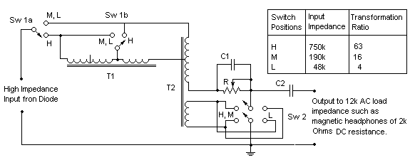
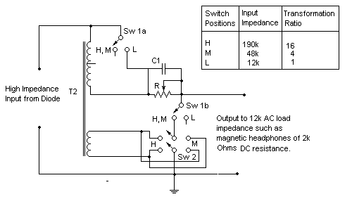
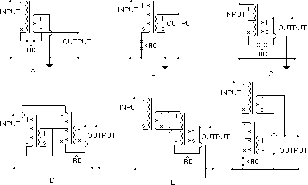
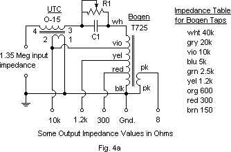
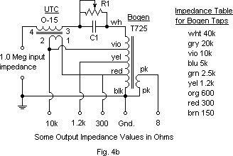
A crystal radio set detector may be simulated in Spice by using a voltage source V1 feeding a parallel tuned circuit L1|C1 through a source resistance R1. The parallel tuned circuit may be made to have any Q by placing a parallel resistor across the tuned circuit. In the simulation circuit files enclosed, an infinite Q is assumed (no RF tuned circuit losses). The actual source loaded Q of the tuned circuit is R1/(Reactance of C1 at resonance). The voltage at the hot end of the tuned circuit is connected through a diode D1 to a parallel RC load R2|C2. The detected output voltage is developed across this load. The purpose of doing this is to enable experimentation to determine how the detection sensitivity changes if the diode type, diode source resistance, and/or load resistance are changed. This program enabled me to develop the graphs shown in Article #1 on my home page that show how detector power loss varies as a function of rectified diode current for a HP 5082-2835 diode and also, more importantly, as a function of diode saturation current Is. The input voltage is modeled as an un-modulated 1.0 MHz sine wave consisting of 4002 individual cycles, sampled at eight points per cycle. If one wants to evaluate the result of using an AM modulated wave, three simulations can be made using min., carrier, and max. Voltage levels of the desired modulated wave. Note: Graphs of diode current and voltage waveshapes, as a function of signal power, may be viewed in Article #8. One of the simulations in the enclosed Zip archive 'Crystal Set SPICE Simulations' (click here) uses a Spice model of a Schottky diode similar to the HP 5082-2835. This is called simulation XtlSetSim1 and its files are contained in the directory XtlSetSim1. The other simulation uses a Spice model of the 1N34A. This is called simulation XtlSetSim2 and its files are in the directory called XtlSetSim2. Each of these directories contains all the files that were generated by my SPICE simulator when I ran each simulation. The diodes used in each of these models have the value of CJO set to 0.0 pF. This does not effect the simulation and makes it easier to experiment with various values of C2 without the detuning effect of CJO. The input source and output load resistance values are equal and match the diode RF input impedance and audio output impedance values. One would expect this condition to give the lowest loss (highest Xtal Set sensitivity) at very low signal power levels. This is not so because at very low input power levels, the diode detector exhibits a square law relation, not linear relation between output and input power. See Article #15 for an explanation of how a theoretical 2 dB increase in detector output can be obtained by a deliberate RF mismatch. In XtlSetSim1 the input sine wave voltage is set to a peak value of 0.1 volts. Since the source resistance is set to 700,000 ohms, the power incident on the detector is -57dBm. The output power delivered to R2 is -68dBm at 10.5 mV. The scale is not shown for the green output curves in the graphs below. That scale is 0.002 mV per division with the zero depressed two divisions below the zero centerline used by the other graphs. A broadcast AM voice signal, if it developed a peak instantaneous power in the detector load of -68dBm, would be just sufficient to enable me to understand about one half the words. This assumes that I am using headphones of an equivalent 700,000 Ohms AC impedance having the power sensitivity of a good real world Sound-Powered Headset. (The 700,000 Ohm impedance, of course would be obtained with the aid of an audio transformer.) The RMS audio power would be about 18dB less or -86dBm. Of course, the impedance values used here are quite high, but they are the values I achieve in my loop crystal radio set. To find out where the -18 dB came from, see Article #1, end of part 1, from the home page. In XtlSetSim2 the input sine wave is set to a peak value of 0.045 volts. Since the source resistance is set to 16,000 ohms, the power incident on the detector is -47dBm. The output power delivered to R2 is -68dBm, the same as in the XtlSetSim1 example. The audio load used is 16k ohms. Note that the insertion loss in XtlSetSim1 is 68-57=11 dB. The loss in XtlSetSim2 is 68-47=21 dB. XtlSetSim1 requires 10 dB less input than XtlSetSim2 for the same output! XtlSetSim1 uses a diode with a saturation current Is=40 nA and n=1.08. XtlSetSim2 uses a diode of Is=2600 and n=1.6. The second graph in article #1 on this site predicts that the loss difference would be 8dB. This experiment illustrates that a detector using a of a lower Is, if it is matched at the input and output, will have a lower loss than one using a diode of a higher Is. I have found, since this article was written, that in a 1N34A germanium diode, the values of Is and n change at low currents. Is may go down as much as 5 times and n may drop 25% from the values used in simulation XtlSetSim2. (Those values were obtained at an unrealistically high diode current of about 320 uA.) This was not expected. The result is that the germanium diode is unfortunately shown incorrectly and in a very unfavorable light (for crystal radio set use). The simulation in XtlSetSim2 probably should have used an Is of about 700 nA and n should have been about 1.15. I used the SPICE program from Intusoft called ICAP4WINDOWS demo version. It can be downloaded for free from their Website at http://www.intusoft.com. The netlists: XtlSetSim1.cir and XtlSetSim2.cir can be edited and used in any other SPICE simulator. Keep the following things in mind:
|
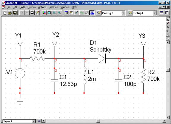
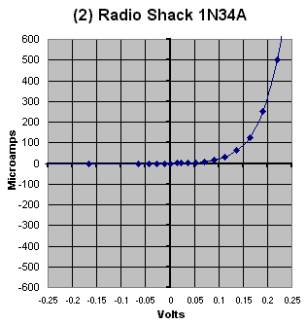
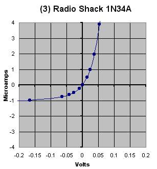
|
Diode Voltage/Current Curves: Does a Specific
"Knee" Voltage really Exist? I think that there is validity to the notion of the existence of a diode "knee" when clamping circuits are considered, and maybe with other circuits. I do not think that there is any validity to the notion of a "knee Voltage" in the forward conduction portion of a diode curve when low signal level detection is considered. The reason is that the apparent Voltage of the knee is an artifact of the Current Scale used in plotting the diode V/I curve. In fact, the shapes of the forward conduction curves of all normal diodes are quite similar, and with no "knee", if the Current scale is logarithmic, not linear. To illustrate this, take a look at the charts below. The first four use a linear scale for the Current axis. The full-scale Current values are: 4000 uA, 600uA, 4uA and 1.25uA. The 1N34A diode is one purchased at Radio Shack with measured Is =2.57uA, n=1.6, and Rs=6.55 ohms. The values of Is and n were calculated from measurements made at an effective diode current of 320 uA. The fifth chart shows the 1N34A and a 1N914 using a linear current scale. The sixth chart shows the two diodes using a log Current scale. The 1N914 has n1.85, Is=2.3nA and Rs=6.0 Ohms. Graph #1 seems to show a knee at about 0.2+ Volts. A knee at about 0.2 Volts seems a little ambiguous in graph #2. In graph #3 the knee has vanished. Graph #4 seems to show a knee on the current scale in the reverse bias region! The fifth and sixth graphs show a comparison of the 1N34A and 1N914 in the forward conduction region with a linear and then a log Current scale. Note the apparent knees on the linear plot and the total absence of any knee on the logarithmic plot. For RF diode detectors to work, one needs a device that
has a non-linear V/I curve. In other words, the slope of the V/I curve
must change as a function of applied Voltage. The slope must be steeper
(or shallower) at higher voltages and shallower (or steeper) at lower
voltages than at the quiescent operating point. To clarify this, look
at curve #3. As a low-level signal detector, this diode will rectify if
biased at -0.025, 0.0 or +0.025 volts. The difference is that the diode
resistance at the -0.025 Volt operating point is higher than that at 0.0
Volts. It is lower at +0.025 than at 0.0 Volts. If one places a
straightedge on the screen of one's PC monitor, tangent to the curve at
-0.025, 0, and then +0.025 Volts, one can measure a slope of about 80k
Ohms at -0.25 Volts, 40k Ohms at 0.0 Volts, and 20k ohms at +0.25
Volts. The rate-of-change of slope as a function of voltage (second
derivative) is less at -0.025 Volts than at +0.025 Volts. This means
that the detection sensitivity when biased at -0.025 Volts will be less
that when biased at +0.025 Volts, even it the input and output are
properly impedance matched.
|
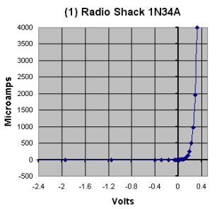
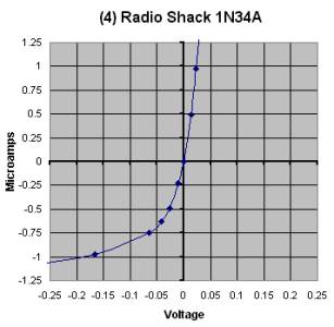
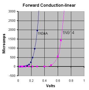
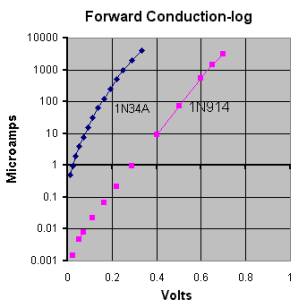
In this article I am going to show an analysis of the operation of a crystal radio set detector using a SPICE simulator. The detector voltage and current waveforms will be shown for three different input "available power" sources. These sources will supply either -85.54, -65.54 or -45.54 dBW (number of dB's below one Watt) power to a matched load. Each power source is made up of a pure voltage source combined with a resistance. (The combo could also be referred to as a "voltage source with an internal resistance"). In each case the available input power, the output power and detector insertion loss will be shown. Conformance to or deviation from the usually assumed peak-detector model will be investigated. The change in input resistance with change in input power will also be examined. Here is a derivation one needs to know in order to understand the rest of this article. The concept of "available power": If one has a voltage source V with an internal resistance R, then the load resistance to which the maximum amount of power (Pa) can be delivered is itself equal to R. Pa will be called the "maximum available power". Any load resistance other than one equal to the source resistance R will absorb less power from the source. This applies whether the voltage is DC or AC (RMS). An equation for power absorbed in a resistance is voltage squared divided by resistance. In the impedance matched condition, because of the 2 to 1 voltage division from the source resistance and load resistance, one-half of the internal voltage V will appear across the load resistance. The actual power absorbed by the load will be, as indicated in the preceding relation: P = ((V/2)^2)/R = (V^2)/(4R). Half of the power delivered to the series combination of the source resistance and the load resistance will be delivered to the load. The other half is dissipated and lost in the source resistance. In the crystal radio set case the input voltage is AC RF voltage. If the input voltage is referred to by its peak value (Vp) as it is in SPICE, instead of by its RMS value, the equation changes. The RMS voltage of a sine wave is equal to the peak value of that wave divided by the square root of 2. Since the power equation squares the voltage, the equation for the "available input power" changes to P = (Vp^2)/(8R). This is the equation that will be used to calculate available input power to the detector, from the source. Here are some definitions, assumptions and explanations:
The Intusoft ISpice netlist shown below is automatically generated by the SpiceNet program after the schematic and parts values are entered into the program. C:\spice8d\Circuits\XSchottky.cir Setup1 Note 1: In regard to the accuracy of the SPICE diode model, some diodes, notably the 1N34A are unusual. The values of Is and n are not constant and do vary with diode current. Measurements made on one 1N34A shows Is and n values of 2.7E-6 and 1.64 at 320 uA which drop to 1.21E-6 and 1.34 at 32 uA, then down to 6.6E-7 and 1.05 at 1.8 uA. Schottky diodes seem to have constant values for n and Is. The SPICE netlist above shows, as the input, a 1.0 MHz
sine wave of peak amplitude 0.125 volts for V1. (This Input signal level
is 2.74 dB less one that would operate the detector half way between the
linear and square law modes. At this lower input signal power level the
insertion power loss of the detector is 7.12 dB). The first of the
three simulations will be done with an input sine wave of 0.125 volts
peak for V1 as shown in the netlist. The second simulation will use a
1.25-volt peak sine wave. The third will use a 12.5-volt peak sine
wave. The respective available input powers are: -85.54 dBW, -65.54 dBW
and -45.54 dBW (dB below one Watt).
The black curve shows the diode current. The other
three curves all use the same scale on the vertical axis. The blue
curve shows the voltage at the test point Y2. This is the voltage
across the tuned circuit. It has a peak value of 61.9 millivolts, about
1/2 that at test point V1. This shows that the detector has an input
resistance of about 700k Ohms. There is a good input impedance match
here. The red curve shows the voltage across the diode. Note that
where it is positive, a forward diode current flows for about 42% of the
time for one cycle of the 1.0 MHz wave. Note that where it is negative,
a reverse diode current flows. This reverse current flattens out and if
a higher input signal was used, it would flatten out at about 38
nanoAmps, the saturation current of the diode. Finally, note that there
is no peak detection going on. The diode output voltage, measured at
test point Y3x is only 15.7 millivolts even though the peak forward
voltage applied to the detector is 61.9 millivolts. Input power as
stated above is -85.54 dBW. The output power is ((0.0157)^2)/700k =
-94.53 dBW. Insertion loss = 94.53 - 85.54 = 8.99 dB.
Here, the input voltage at test point Y1 is 1.25 volts,
but the voltage across the LC tank circuit, as measured at test point Y2
is only 494 millivolts, not 625 which would be the case if we had a
perfect impedance match. This shows that the detector input resistance
is now lower than 700k Ohms. Diode operation is getting closer to peak
detection. The green output voltage at test point Y3x is 361 millivolts.
Forward current is now drawn over about 24% of one cycle time. The
input available power, as stated
Now it looks as if we are getting much closer to peak detection. The peak positive voltage applied to the diode at test point Y2 is 4.30 volts. The detected DC voltage at test point Y3x is 4.08 volts (only about 5% less than the 4.30 volt peak). The diode forward conducts only during about 12% of the cycle time of the 1.0 MHz wave. As stated before, the input available power is -45.54 dBW. The output power calculates as: ((4.08)^2)/700k = -46.23 dBW. Detector power loss goes down to: 46.23 - 45.54 = 0.69 dB. The input resistance is now even lower than before. The green output voltage at test point Y3x is 4.08 volts, kind of low compared with the 6.25 volts we would get with a perfect input impedance match. Why is this? The input and output resistances of a diode detector both approach the value (0.026*n)/Is Ohms at low signal power levels. (n and Is are diode parameters used in SPICE. n is called the diode Ideality Factor, or Emission Coefficient. Is is called diode saturation current.) Is is defined as the current that is asymptotically approached in the diode back bias direction before extraneous leakage factors or reverse breakdown comes into play. It also has a major effect at an on the amount of current a diode will pass in the forward direction at any specific applied Voltage. As we have seen, as signal input power increases, the quality of the RF impedance match starts to degrade. The AC input resistance to the diode detector decreases from the value obtained in the first well matched low power level simulation. Interestingly, the output resistance increases. The reason for this change is that a new law now governs input and output resistance when a diode detector is operated at a high enough power level to result in a very low power loss. The rule here is that the DC input resistance of an ideal diode peak detector is one-half the value of the output load resistance. Also, the output resistance is equal to two times the value of the input source resistance. Further, since in this example the detector now approaches being a true peak detector, the DC output voltage approaches the square root of 2 times the value of the RMS input voltage. This relationship is necessary in an ideal peak detector so that the AC input power can equal the DC output power with no power lost in the diode (No free lunch). If we were to restore an optimum impedance matched condition by adjusting the input source resistance to 495k ohms and the output load resistance to 990k ohms (by changing the input and output impedance transformation ratios), the power loss would be further reduced to 0.22 dB. See Part 5 of Article #0 for further discussion on the subject of input and output resistance of diode detectors operated in their peak-detection mode. |
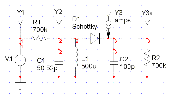
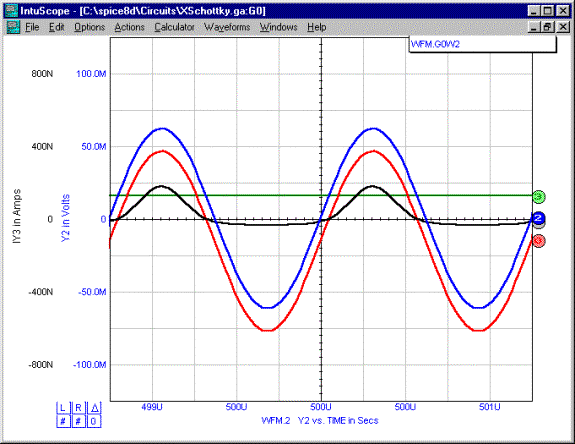
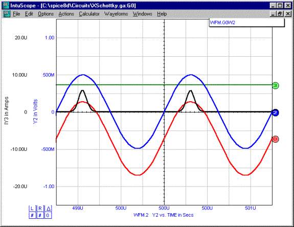
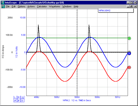
|
Build the Diode Detector Bias Box: a simple and easy way to determine if one's diode is optimum for weak signal reception, or should have a higher or lower axis-crossing resistance (0.026*n/Is ohms)
Quick Summary: The 'Diode Detector Bias Box' enables one to check whether the diode being used in a crystal radio set has optimum characteristics for that set. The optimum detector will deliver the greatest low-signal sensitivity. A detector diode, in order to deliver the highest sensitivity and lowest distortion, must be properly impedance matched to its RF source. It must also be matched to the correct (for that diode) audio and DC load resistances. See Articles # 0, 1, 5 and 15a for more info on this subject. How can one know for sure that the diode used in one's own crystal radio set is the best one for it? Another way of putting it is: Does my diode have the Saturation Current (Isopt) that the optimum diode, for my set, would have? An easy way to find the answer is to build and use the diode Detector Bias Box.
To change the detector performance of a diode of Is = Isor (original) to the performance of a diode of Is = Isop (optimum), a DC bias voltage must be inserted in series with the diode. The required bias voltage is: Vbias = 0.0257*n*[ln (Isop/Isor)]. ln represents the natural logarithm of the expression following it. This equation is accurate if the values of Is and n do not change as a function of diode current. This assumption is correct for the Schottky diodes I have checked. Some germanium ones I have checked do not accurately follow the Shockley equation. They tend to have high values of Is such as 500 nA or more. Germaniums having Is values in the 100-200 nA range do seem to follow the Schockley equation well. At high currents, Is increases from its value at low currents. The Vbias equation is given for information only and is not used in the following experimental procedures. Whether a Schottky, germanium or other diode is used, a convenient way to 'tune' the Is of a diode is to use the "Diode Bias Box". It effectively enables one to change a diodes' effective Is (and therefore its operating impedance) by merely turning a knob on a box. The Diode Bias Box also enables one to determine the best diode DC and AC load impedance. Here is an interesting relationship that applies to most Schottky diodes: A Shottky diode detector having a saturation current of (Is1) that has no external DC current bled into it will perform, as a diode detector, identically to that of another diode having a saturation current of (Is2) if a DC current (Ib) equal to (Is1-Is2)of is bled into it. To use the Bias Box, connect the terminals labeled T1 to the crystal radio set ground and the cold end of the audio transformer primary, if one is used. If no transformer is used, connect the terminals of T1 to the crystal radio set ground and the cold end of the headphone headset. Also make sure that the connection where the Bias Box is inserted is well bypassed for RF and audio. To operate the box, snap the switch to OFF, disconnect the Hot T1 connection from the crystal radio set and adjust the DIODE DC LOAD pot to the DC load desired (See articles #1 & 4 or pick 100k Ohms to get started). The DC load resistance can be measured across the terminal strip labeled T1 when its hot lead is disconnected from the crystal radio set. Reconnect the Hot T1 connection to the crystal radio set DC return. Tune in the weakest station you can copy. Snap the switch to ON. Adjust the BIAS pot for the the greatest volume. Tune in the strongest station you can get. Adjust the DIODE DC LOAD pot for the least audio distortion. Disconnect the antenna. Connect a DVM to terminal strip T2. If you find a voltage there, that is an indication that your diode is not optimum. A diode having a different Is could work the same, but without the need for any bias. If your diode is biased in the forward direction, the optimum diode would have a higher Is than your present diode. A reverse bias indicates that the optimum diode would have a lower Is. As stated before, the relationship between the required bias (Vbias), the Saturation Current of the original diode (Isor) and the Saturation Current for the optimum diode (Isop) is: Vbias = 0.026*n*ln(Isop/Isor) volts. Some illustrations: To change Is by five times, the bias Voltage required is about 0.044 Volts. To change it by 25 times, the Voltage is about 0.088 Volts. Note: When adjusting the BIAS pot from the optimum position, moving toward forward bias reduces volume, sensitivity and selectivity. Moving toward reverse bias increases selectivity, reduces volume and sensitivity and adds audio distortion. What to do now? If the optimum diode has a higher Is than your present one, several identical diodes can be paralleled to create the equivalent of one of higher Is. For instance, five in parallel will have an Is five times that of one alone. If you have several different diodes, experiment with them. Maybe you can find one that does not need a bias for best results. In recent years many different types of diodes called 1N34A have been sold. Their Is values vary all over the lot. Some final comments: Using the Bias Box to reduce the effective Is of a diode that has a high Is does not work very well if a large reduction is needed. The reason is that diodes of high Is naturally have higher back leakage and a lower reverse breakdown voltage. This causes losses and distortion when the RF voltage across the diode swings to reverse polarity every RF cycle. Less sensitivity and selectivity is the result. When one increases the effective Is of a diode that has a low Is by applying a forward voltage bias, this problem does not occur. Some other things that will cause some optimized diodes to work worse than others are: High series resistance (Rs), high diode barrier capacitance (this reduces high frequency performance compared to that at lower frequencies) and high reverse leakage current. |
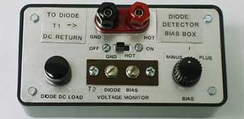
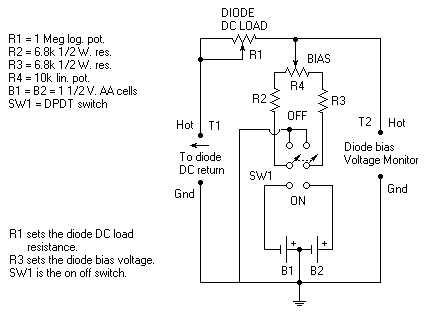
| A New Diode Detector Equivalent Circuit, with a
Discussion of the Linear-to-Square-Law Crossover Point: the signal level
at which the detector is functioning midway between linear and
square-law operation Quick Summary: The purpose of this article is to describe and and then compare a new diode detector equivalent circuit (DDEC) to a real world detector circuit (RWDDC), such as might be used in a crystal radio set. This equivalent circuit uses an ideal diode. Comparisons are made using SPICE simulations of the two circuits. Calculations using equations given in Article #15A are also supplied for comparison. The concept of the Linear-to-square-law crossover point (LSLCP) in the relation between output DC and input AC power is introduced (not to be confused with the exponential relationship of DC current to DC voltage in a diode). Part 1: General Description of a Diode Detector. The new diode detector equivalent circuit (DTEC) is based on the idea that a detector diode imbedded in a proper circuit can be thought of as a 'black box' device that converts RF power into DC power. Some power is lost in the process and that is called Diode detector insertion power loss (DDIPL). This approach completely avoids such concepts as duty cycle, pulse current, bypass capacitor charging and non-linear instantaneous voltage/current relationships. It is also consistent with the material given in Article #1. The peak-detector, capacitor-charging-current line of thought is good when signal levels are high enough to assure that true peak detection occurs. It is not very useful when signal levels are low. However, when all is said and done, the more different valid ways one can use in thinking about how a circuit works, the better becomes one's understanding of that circuit. This analysis applies to an AM detector fed by a CW RF sine wave voltage of frequency fo: It has a peak (not RMS) value equal to V1 and an internal source resistance of R1. The "maximum available RF input power" is called P1 (see section 2 in Article #0 for info on "maximum available power"). The DC output power delivered to the load resistor R2 is called P2. The DDIPL (in dB) is equal to ten times the log of the ratio between the two powers P2 and P1. This approach can also be used to model how a diode detector behaves with an AM modulated input signal by performing a SPICE simulation three times. Once with the RF signal equal to the value of the desired modulated wave's envelope minimum value, once with the signal equal to the carrier value and once with the signal equal to the crest value. The three DC output voltages give the minimum, carrier equivalent and peak value of the demodulated output audio wave. ***** Please do not skip this next paragraph! ***** To understand the new diode detector equivalent circuit, one must abandon the usual way of thinking the about the diode in a detector. Instead, one must think about the "diode detector circuit". This circuit includes a tank circuit T, the output capacitor C, as well as the diode. The shunt input reactance of the circuit is assumed to be zero at all frequencies except fo, the frequency to which the tank is tuned. The input resistance at fo will be discussed later. The output reactance of the circuit is assumed to be zero at all RF frequencies. The output resistance will be discussed later. A real world diode is a two terminal device. The "real world diode detector circuit" will be modeled as a "two port, four terminal device" having a pair of terminals for the input and another for the output. One of the input terminals is the "hot" input terminal; the other is "low". One output terminal is the "hot" one, the other is "low". The two "low" terminals are connected together and usually to ground. Please note, that in the topology of the two schematics shown below, the "Diode Detector Circuit" and the "Diode Detector Equivalent Circuit" both include the tank T and the bypass capacitor C2 as an integral part of the detector. Also, look at the circuits in this way: The tank circuit, looking towards the output, sees the diode as a one-end-grounded shunt load since the output bypass cap is a short at RF. The output load resistor, looking back towards the input, sees the diode as a one-end-grounded shunt DC resistive source since the input side of the diode is shorted to ground by the tank. See Fig 1. The detector tank circuit T is modeled as lossless and resonant to the input frequency fo. Losses in a real world tank can be accounted for by using Thevenin's Theorem to calculate the appropriate changes in V1 and R1. This leaves the circuit topology unchanged. See Article #1 for more on this subject. The value of the tuning capacitor in T is sufficiently large so that essentially no harmonics of fo can appear across T. This assures that the "pendulum-like resonator effect" of a high Q circuit will be available to supply the narrow, high-current pulses the diode requires every cycle when strong signals are handled. Another advantage is that tank-voltage-waveform peak clipping by diode conduction is essentially prevented when the current pulses are drawn. All this assures that the input impedance to the detector will be linear over one cycle of RF and the input current to, and voltage across the tank T will always be sinusoidal, no matter how weak or strong the input signal. See Article #8 for an illustration of typical waveforms. A reactance value for the tank capacitor equal to less than one hundredth of the value of R1 will be sufficient. The DC resistance of the tank inductor should be small enough so that no appreciable DC voltage will appear across it. A value less than one hundredth of the value of R2 will be sufficiently small. This assures that all of the output DC power goes into R2. The bypass capacitor C2 has a very low reactance compared to the load resistor R2 at the frequency fo. Since C2 acts as a short circuit across R2 at the frequency fo, all of the RF voltage across T will appear across the Diode. The time constant, R2*C2 should be long compared to the time for one cycle of fo. Part 2a: Discussion of the new Diode Detector Equivalent Circuit.
To gain an understanding of the Diode Detector
Equivalent Circuit (DDEC), first consider the following line of
thought: See Fig. 1. Let the input RF voltage V1 become very low.
V1, at a frequency fo, looking toward the load resistance R2, will see
an RF resistance (at fo) equal to the junction resistance of the diode
at zero bias. At this very low signal condition the detector input
resistance is not affected by any changes made to R2. The value of this
junction resistance is the slope of the diode V/I curve at the origin.
From a differentiation of the ideal diode equation, the numerical value
of this resistance is: (0.0256789*n)/Is ohms at a temperature of 25
degrees C. Let's call this Ro. Is and n are parameters in the ideal
diode equation. (For a discussion of Is, n, etc., see the text after the
schematics in Part #1 of Article #1). From the load resistance R2,
looking back toward the input, one sees the same resistance value Ro,
and it is independent of any changes at the source. Now look at Fig.
2. Here, the real world diode has been changed to a theoretical ideal
diode and two attenuators, A1 and A2, of characteristic resistance Ro
have been are added. If V1 becomes zero, the attenuators A1 and A2 must
be set to infinite attenuation to enable the model to duplicate the
behavior of the circuit in Fig.1. When an input signal is applied, the
values of A1 and A2 must become finite. The DDIPL is equal to the sum
of the loss of each attenuator plus the impedance interface loss between
the ideal diode Di and each attenuator, as well as any mismatch loss
between R1 and the detector as well as between R2 and the detector (See
** after Table 2). SPICE simulation shows that the diode detector
equivalent circuit does a pretty good job modeling the operation of a
real world diode detector. To verify this, one can perform a SPICE
simulation of Fig.1 and Fig. 2 with V1, R1 and R2 the same in each
case. The attenuation value of A1=A2 dB must be set to a value that
causes the output, V2, in Fig. 2 to be the same as in Fig.1. The input
impedance match of the two simulations differ from each other by less
than 14% over an input power range of 48 dB, centered at the
Linear-Square-Law Transition (LSLCP) point. This is the main area
where the results from the DDEC simulation differ from those of the RWDD.
The input resistance of the DDEC is always higher than that of the REDD.
This equivalent circuit seems to work for signals from well below the
LSLTP point up to levels just before "Diode Reverse Breakdown
Current" comes into the picture.
Fig. 2 Some definitions and conditions that apply to Fig. 2 follow:
Table 1 shows three groups of data: SPICE simulations of the RWDDC and the DDEC, and a set of calculated values from equations appearing in Article #15A. Data is shown for three input power levels for each data group The levels are: 1) The input power that will operate the RWDDC at its LSLCP [Plsc(i)], 2) 1/128 the value of Plsc(i), and 3) 128 times the value of Plsc(i). These power levels are believed to be correct if the input and output impedances of the detectors are impedance matched, using appropriate values for R1 and R2. Actually, in the simulations, R1=R2=Ro=0.0256789*n/Is. This causes the required input power for the desired output to be somewhat greater than if input and output were perfectly matched. The attenuators A1 and A2 in the DTEC are set equal to each other, and to a value that causes the output power of the DDEC to closely equal that of the RWDDC. SPICE parameters for the diode in the RWDDC and "Calculated values" are: (Is)=38 nA and n=1.0*. The "calculated values" assume impedance matched conditions. The SPICE circuit simulation program "ICAP/4" from Intusoft was used in all simulations.
* The n of real world diodes is never 1.0. Actual values of good detector diodes are usually between 1.03 and 1.10. The input and output power values given in the data group for the RWDD can be corrected if n is over 1.0 by adding 10*log (n) dB to the P1 and P2 figures. Keep in mind that n and (Is) are most always independent of current for Schottky diodes. This is not the case for silicon pn junction or germanium point contact diodes. A New diode detector equivalent circuit, with a discure law crossover point. *** Calculations for a RWDDC using equations #6 and *2an given in Article #15A. These equations assume perfect impedance matching at the input and output. Part 2b: An alternative DDEC. An alternative 'diode detector equivalent circuit' (DDEC2) can be formed by moving the tank circuit T from its position shown in Fig. 2 to the left hand terminal of diode Di and moving the bypass capacitor C2 to the right hand end of resistor Rs. This equivalent circuit always operates as a peak detector, so no 'excess loss' need be accounted for. The loss for attenuators A1=A2, at any input signal level may be calculated from equations #3n and #6 in Article #15A. Loss for A1=A2=5*log(DIPL from equation #3n) dB. The input impedance (S11) of the DDEC2 approaches that of the RWDD at high and low input power levels. Its input resistance at intermediate power levels is always lower than that of the RWDD. Part 3: Further Discussion of the Linear-to-Square-law Crossover Point. The RF input resistances in the simulations of the DDEC (Fig.2) are within 17%, 17% and 8% at the low, medium and high power inputs respectively, of the simulated resistances of the RWDC (Fig 1). The DDIPL values at each input power level for the circuits in Figs. 1 and 2 were set to within 0.1 dB of each other by adjustment of the loss in A1 and A2. Operation at the LSLCP: Operation at the LSLCP can be said to occur when the detector is operating half way between its linear and square law response mode, the point where the two areas overlap equally. At this point there is a sqrt(2) dB change in output power for every 1.0 dB change in input power. Operation at power levels below the LSLCP point: As input power levels are lowered, the DDIPL approaches 10*log{[I2/(I2 + Is)]}-6 dB. Operation at power levels above the LSLCT point: Here, the DDIPL tends to approach zero, but the detector input and output impedance match starts to deteriorate. This is the regime where the mode of detection changes from "averaging" to "peak". (See Article #0, Section 5 for an explanation of this effect.) Re-matching the input and output circuits at these higher input RF power levels recovers the excess loss caused by the mismatch, and results in the performance given by the equations in Article #15A. Input/Output impedance interaction: When an input signal is present, interaction between the input and output circuit occurs. That is because the attenuation of the attenuators A1 and A2 must become finite and that lets the interaction come through. If the output load R2 is reduced, the input resistance to the detector will be reduced. If the input source resistance R1 is reduced, the output resistance of the detector will be reduced. This interaction is dependent on the strength of the input signal. For greater input signals, there will be less DDIPL (Lower values for attenuators A1 and A2) and greater interaction. If DDIPL approaches zero, the output resistance will approach two times the source resistance R1. Similarly, the input resistance will approach 1/2 the load resistance R2. If the input signal power is reduced, detector input and output resistance values become decoupled from each other and both approach Ro. See the paragraph below Fig. 1. Overview: One can think of a diode detector circuit as a device to change input RF power to an almost equal amount of DC output power, provided the input power level itself is high enough. In this instance the attenuators A1 and A2 in Fig. 2 have very low values. If the input power is reduced, A1 and A2 increase in loss, thus reducing the output power. At low input power levels, square law operation occurs. In this region, if the input power is reduced by, say, 1 dB, the loss in attenuators A1 and A2 are each increased resulting in an output reduced by 0.5 dB. Voila, square law operation! There is an extra loss besides that of A1 and A2. It is the interface mismatch loss between each attenuator and the diode Di as well as input and output mismatch losses. This interface loss varies as a function of input power. It is about zero when the values of A1 and A2 are very low (large signal power condition) and approaches 3 dB for each attenuator at low signal power levels (total of about 6 dB). See the Table 1 above and the ** comment below it. |
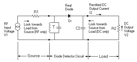
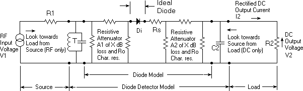
Power Loss), Selectivity and Input/Output Impedance of a Crystal Radio Set
Quick Summary: This Article describes a device and procedure for quantifying several characteristics of crystal radio sets. They are: (1) Insertion power loss, (2) Selectivity, (3) RF input impedance match and (4) Audio output resistance. First, an acknowledgement: This article was inspired by
a paper written on 9/15/99 by Charlie Lauter at: Lautron@aol.com . It
can be accessed at: http://home.t-online.de/home/gollum/testing.htm .
He led the way with a good procedure for sensitivity and selectivity
measurement, but I wanted a more general approach. Here is mine:
This article is divided into six sections. The first describes the IPL (Insertion Power Loss) measurement method. The second gives a theoretical derivation. The third shows a method for the measurement of selectivity. The fourth shows how to measure the input impedance match of a CSUT (crystal radio set Under Test). The fifth shows a method for measuring the output resistance of a crystal radio set. The sixth gives some comments and suggestions on how to improve crystal radio set performance. A quick definition: The IPL of a crystal radio set may be loosely defined as 10 times the log of the ratio of the audio power delivered to the output load divided by the maximum RF sideband power available from the antenna. Here comes a more rigorous definition of IPL: The function of a crystal radio set is to convert (demodulate) the modulated RF signal sideband power received by the antenna-ground system and deliver as much of that power as possible to the output load as audio output power. Understand that all of the signal information modulated on a carrier and picked up by an antenna-ground system resides in the power carried in the sidebands of that signal. No signal information is contained in the RF carrier. The Insertion Loss Method assumes that a voltage source with a specific internal impedance is connected through a "device under test" (DUT) to a load resistor. We can say that the DUT is "inserted" between the source and the load.
Now, a brief detour to explain the concept of MAP (Maximum Available Power) and a more detailed look at Insertion Power Loss (IPL) as used in this Article. Maximum Available Power (MAP)
Here is how to calculate MAP from the Vs and Rs combination. As mentioned before, the maximum power output occurs if Rl = Rs. This means that the total load on Vs is the series combination Rs + Rl = 2*Rs. Since power in a resistor can be calculated as (V^2)/R, the total power dissipated in the two resistors is (Vs^2)/(2*Rs). Since one half of the power is dissipated in Rs (and lost) and one half in Rl, the maximum power deliverable to Rl is: (Vs^2)/(2*Rs)/2 = (Vs^2)/(4*Rs). We will use this relationship later on. Note that Vs^2 means Vs squared and 4*Rs means 4 times Rs. Vs is in RMS volts. If Vs is given in peak or peak-to-peak units, a correction factor must be applied. Definition of IPL when the input signal is an RF
carrier, modulated by a sine wave. Output power and IPL: Assume that an RF source with a MASP of Pa Watts is connected to a CSUT and that the CSUT feeds a load resistor. The source has an internal RF impedance of Za Ohms and the load has an impedance of Rl. The SCUT is tuned and adjusted to deliver maximum audio power to the load, with the desired selectivity. Define the output power as Po. Now imagine the replacement of the CSUT with an ILCS. It provides a perfect impedance match to the source and perfectly matches the load. Its output power will equal Pa because there are no losses. This ideal crystal radio set will function as a device to convert all of the MASP into audio power. The ratio of the output power of the CSUT to that of the ICS set is Po/Pa. This ratio, expressed in dB is the IPL of the CSUT. IPL = 10*log (Po/Pa) dB. The load resistor should have a value equal to the average impedance of the headphones to be later used with the CSUT. (See Article #2 on how to measure headphone impedance.) Section 1. IPL Measurement Method.
It is assumed that by tuning the CSUT for maximum output volume, that the best conjugate impedance match possible is presented to the antenna. In simpler terms, tuning for maximum volume adjusts the resistance component of Zi to as close to 25 Ohms as possible and the reactive component of Zi to as close a value as possible to the negative of the reactance of La and Ca in series. This set of circumstances transfers the most signal power possible from the antenna to the CSUT. The test procedure that follows involves applying a modulated RF Voltage (Ea) through a dummy antenna to the input of the CSUT and then measuring the Audio Output Power (Po) delivered to the output load. The IPL of the CSUT is calculated as: IPL = 10*log (Po/(MAP in the sidebands of Ea)). Measurement of IPL
We will use use a special attenuator box between the SG and the CSUT and call it the AMCS. Refer to the schematic in Fig. 2. The AMCS has one 3 dB and one 20 dB attenuator that are used in measuring selectivity. It has an additional 10 dB attenuator in the event some extra attenuation is needed. The 20 dB attenuator can also be used to determine the voltage Ea at test point P1 when it is so low that it is hard to read. The series 45.0 and two parallel 11.1 Ohm resistors form a "minimum-loss impedance transforming attenuator". Its input design resistance is 50 Ohms. Its attenuation is set so that the ratio of the voltage at test point Pi to that at P1 is 10:1 when Sw1, Sw2 and Sw3 are set to zero dB. The source resistance feeding the Dummy Antenna and crystal radio set series combination is 5.25 Ohms. Two 11.1 Ohm resistors are used in place of one of 5.55 Ohm resistor because resistors under 10 Ohms may be hard to find. This also minimizes lead inductance. If the 45.0 and 11.1 Ohm resistors are held to within +/- 4%, the attenuation accuracy will be within +/- 0.33 dB. of nominal. Resistor accuracy tolerances for the other attenuators, to hold a +/- 0.33 dB accuracy are: 3 dB-10%, 10 dB-4% and 20 dB- 2.5%. The load on the CSUT must be a resistor (R1) of value equal to the effective impedance of the headphones used with the crystal radio set. One can determine the impedance of the headphones by building and using the FLVORA described in Article # 2. Alternatively, it may be estimated as 5 or 6 times the DC resistance of the phones. To measure the IPL of a crystal radio set, connect the SG**** to the AMCS and set it to a test frequency of, say, 1.0 MHz. Turn on the sine wave modulation function and adjust the frequency to 1000 Hz**** and the modulation percentage to 50%****. (50% modulation exists when Ea_pp is three times Ea_vv.) Connect the AMCS to the antenna and ground terminals of the CSUT. Connect the scope to Rl and set it to a sensitivity of 2 mV/div. Set the SG to a high RF output and tune the CSUT to maximize the 1000 Hz trace on the scope****. Reduce the SG output as necessary to keep the scope trace on scale****. Reset the SG to deliver a 4 mV p-p trace on the scope. Connect the scope to point P1 and measure and record Ea_pp and Ea_vv at Point P1.
Here are the labeling conventions that will be used. Voltages on the input side of the CSUT always start with Ea. Voltages on the output side start with Eo. The underscore is a separator from the description suffix that follows. fo = carrier frequency, fmod = modulation frequency, pp = peak-to-peak, vv = valley-to-valley, car = carrier, dc = direct current, sf = side-frequency, carpp = carrier peak-to-peak, 1sfpp = one side-frequency peak-to-peak, 1sf = one side-frequency, 2sf = two side-frequencies.
The IPL of any crystal radio set depends upon the output power level at which it is operating. At very low output levels (signal barely readable with sensitive headphones), the IPL increases about 6 dB for every 6 dB reduction in input power. This results in a 12 dB reduction in output power. When this happens, the diode detector is said to be operating in its "square law region". Because of this effect, it is suggested that the IPL be measured at several audio output power levels when characterizing a crystal radio set, maybe -80 and -110 dBw. Section 2. Derivation of IPL. The output waveform shown in Fig.3 is a sine wave Eo_pp, having a DC value of Eo_dc. The audio power it supplies to the output load Rl is: Po = ((Eo_pp/(2*sqrt2))^2)/Rl. The "2" and the "sqrt2" are needed as before to change Eo_pp from a peak to peak to an RMS value. Simplifying, Po = ((Eo_pp)^2)/8*Rl. Since IPL = 10*log (Po/MAP_2sf), and we can state the Final Result we've all been waiting for, and it is: INSERTION POWER LOSS = IPL = 10*log {32*Ra*[(Eo_pp/D)^2]/Rl}. There is one caveat to using this method: It is assumed that the audio bandwidth through the audio transformer, as well as one half the -3 dB bandwidth of the RF tank is 3 or more times as large as the recommended 1000 Hz modulation frequency. If both are 3000 Hz, the error will be about 0.6 dB. I either of these bandwidths is too small, a lower modulation frequency such as 400 Hz can be used. The MAP of the RF carrier only from the AMCS to the CSUT is: ((Ea_pp + Ea_vv)^2)/(3200) Watts. Section 3. Measurement of Selectivity Shape
Factor: Section 4. Measurement of Input Impedance Match
Section 5. Measurement of the Output Resistance
(Ro) of a Diode Detector. Section 6. Comments.
|
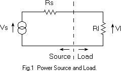
First off, understand that I am not an antenna engineer and present these speculations to suggest a way to increase the directive gain of a small (compared to a 1/4 wavelength) antenna. For simplicity of discussion, wave propagation issues will not be delved into. We will consider that the operation of an inverted L antenna results from the sum (superposition) of two modes of operation. The first mode is that of a capacitively loaded vertical antenna. See Fig. 1. Co represents the "top hat" loading capacity. Visualize the horizontal wire BCD shifted to the left so as to be symmetrical relative to the downlead AB (with point C of ABC directly above vertical downlead BA). The total capacitance, Co, of wire BD to ground acts as the top hat capacitance for the "vertical antenna" downlead BA (the additional capacitance between the upper and lower parts of down-lead BA can be ignored because the antenna is assumed to be short compared to 1/4 wavelength). The second mode is as single turn 'virtual loop' antenna. Let X represent a crystal radio set with antenna and ground connections, a and g. Fig. 2 shows Co as a lumped capacitor C1, connected to ground at the center of the BCD horizontal element. The rectangular loop circuit ABCFG, consisting of the four sides AB, BC, CF and FG can be looked at as a single turn loop antenna of area A, oriented to pickup signals from the B<->D direction. Note that the path for the 'displacement current' through C1 makes up one side of the loop. The current flowing from the induced EMF in the loop will combine to current from the EMF picked up in the down lead BA. These two EMFs add when a signal comes from the direction opposite to that to which the open end points and tend to cancel when coming from the opposite direction. This gives a plausible explanation of the mild directivity of the inverted L antenna. This directivity has been theoretically demonstrated by using computer simulation. For clarity, Fig. 3 shows a top view of the antenna. The following changes to the configuration may serve to increase the directional gain of the antenna (I haven't tried them out.). The induced voltage in a loop antenna (small compared to a wavelength) is proportional to its area, among other things. If the effective location of capacitor C1 could be moved to point D, and its value kept the same, the area of the loop would be doubled to 2*A (ABDEG), thus doubling the current from its induced EMF and further increasing the directive antenna gain. Let us change the lumped representation of Co as one capacitor C1 into two capacitors, one from point B to ground and the other from point D to ground. They will each be equal to one-half of Co and both still will act as a top-tat capacitor for the vertical antenna BA, otherwise known as the lead-in. The one from D to ground will be called C2. See Fig. 4. One way to add more capacitance to ground at point D is to construct two lateral arms on the antenna. See Fig. 5. If each arm is the same length as one half the horizontal element BD (They can be of some other length.), the effective capacitance they add at point D is 2*Co/2=Cadded. The sum of the two capacitors C2 and Cadded is 1.5*Co = C4. The loop area is doubled and the current from the induced EMF is tripled (because C3 is one and one half times C1). The antenna directivity may thus be increased giving more gain in the direction in which the two effects add, and less in the opposite direction. If the directive effect can be made strong enough, a cardioid pattern should result, with a good null in the "opposite" direction. A more practical approach might be to have the two side arms droop down at an angle and be secured to ground with insulated guy wires. A single vertical wire, similar to the lead-in, might work as a substitute for the two arms if its bottom end does not get too near the ground (inverted U antenna). Note there is no "free lunch" here. To the extent that the signal pickup is increased in the direction opposite to that to which the open end points, it is reduced in the other direction. |
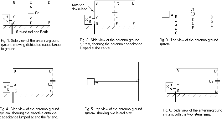
Quick Summary: This Article describes a device and procedure for measuring the sensitivity of earphone elements. Its purpose is to provide a quantitative method for comparing elements. Elements may be easily sorted for application to listening to weak signals, as in crystal radio sets. Actual measurements of an assortment of elements is provided. The Transduction power loss of a headphone element can be defined as the ratio of its output acoustical power to input electrical power. We will call it HPEL and express it in dB. A convenient way to measure HPEL is to use one element of a pair of identical headphone elements as a speaker and the other as a microphone, acoustically couple them together and then measure the input electrical power to the speaker element and the output electrical power from other element. Ten times the ratio of the log of the ratio of output to input power is the transduction power loss of the combination of the two elements, in dB. If the two elements are identical, the power loss of each is one-half that figure. Here is a step by step procedure:
Figure 2 shows the circuit of a bandpass filter having
-3 dB points of 0.3 and 3.36 kHz with a loss of 0.4 dB at 1.0 kHz. It's
powered by a common 9 V. battery. Since the typical 1000 DC Ohms
magnetic earphone element has an impedance of 6000 Ohms and the typical
balanced armature sound powered magnetic element has an impedance of 600
Ohms, approximations of these two resistance values are included in the
switched resistive output controlled by S1. An IC suitable for the
circuit is an LF353 or an MC34002.
A convenient source for white noise is the headphone
output of a small FM/AM transistor receiver, switched to FM and tuned to
a point on the dial where it receives no signal, just noise. The noise
density is rolled off at 6 dB per octave above 2.1 kHz by the
de-emphasis filter in the receiver, but this should make little
difference in the results. The acoustic coupler used to couple the two
elements under test is based on the ANSI 9-A earphone coupler. See
"Acoustic Measurements by Leo Beranek, pages 743 and 744". An
approximation to the ANSI 9-A coupler can be made of a piece of 1"
nominal diameter, medium weight copper tubing having a #120 O-ring glued
on each end. The length of the copper tube used is 0.26 inches. The
I..D. of the O rings is specified as 0.987" and thickness as 0.103". 1"
copper tubing is specified to have an I.D. of 1.025 and an O.D. of
1.125". The total enclosed volume is about 6 cubic cm. An alternative
coupler that may give similar results is a stack of eight or nine 1/8
inch thick garden hose washers having an ID of about 5/8 inches. The
ANSI 9-A coupler is (was?) the standard coupler used in Audiometry when
calibrating an earphone element with a standard microphone. It is a
greatly simplified version of a model of the human ear canal with an
earphone cushion pressing on it. Comments: The DVM should preferably be an RMS responding instrument. The typical DVM responds to the full wave rectified average signal and will probably be satisfactory. Don't use a meter that responds to the peak or peak-to-peak value of the AC signal.
* One of the RCA/GE units was about 6 dB less sensitive
than the other. Thanks to Dieter Billinger (sky_wave_99), I knew that
some RCA/GE elements having low sensitivity could be improved by
sticking a small neodymium magnet to the outside of the case. It worked
in this case, increasing sensitivity of the weak element by 6 dB, so it
was somewhat more sensitive than the other element. BTW, a magnet could
not increase the sensitivity of the other originally more sensitive
element. These two units appear to be of somewhat different
construction. To easily compare the power sensitivity of any two
elements, even if they differ widely in impedance, see Article #3. To help in understanding these charts, consider that an eight dB (6.3 times) change of power is usually perceived as a two times subjective change in loudness.
2. Comparisons In order to compare the sensitivity of headphone
elements that are used flat against the ear, as well as those that are
not, (but are inserted into the ear canal (tips) or outer ear (buds)), I
decided to make one of my best elements a "standard" and compare the
others to it using a DFLVORA (see Article #3). That "standard" is a
Western Electric Sound Powered receiver element # D173012 held flat
against one ear. In the results shown below, two Mouser elements were
tested and found to be of equal sensitivity. (That was after I found
one Mouser to be weak until I whacked it several times.) The two Radio
Shack units also tested equal. Note that the DFLVORA can be used to
easily compare the power sensitivity of any two earphone elements even
if they differ greatly in impedance. For more information, see the
next-to-last paragraph in Section 1 of Article #2.
These comparisons were made using a voice signal from a small transistor radio fed into a DFLVORA with the radio volume set to a level at which I estimated I could understand about 50% of the words. Results may differ for people who are not old and do not have poor high frequency hearing, such as myself. The differences in tone quality between the standard element and a DUT will have a different effect on intelligibility for different people. The sensitivity values for the piezo electric elements can only be attained if the elements do not have a resistor placed across them to supply a DC path for diode detector current. The resistor adds loss (although this is a low cost approach to provide a DC path for the diode current). Also, if the resistor is made large in order to reduce its loss contribution, audio distortion will oftentimes take its place. The best way to drive the elements is to use an audio transformer to impedance match the diode detector output resistance to the average impedance of the element. The transformer supplies supply a DC return path for the diode. A further advantage of using a transformer is that no DC voltage can get across the piezo element. Sometimes, if a strong signal is tuned in and it produces a large rectified DC voltage on the element, the element will "freeze" and its sensitivity will drop. See Article #5 for info on transformer coupling and diode DC resistance loading. (The value of the DC load resistance on the diode should equal the average value of the AC audio load impedance.) * The comparison of the sensitivity of an element in a series connected element pair DUT with the "standard element" was made in the following manner: The full (two element) headphones DUT was connected to the J1 output of the DFLVORA. The DFLVORA was fed by a weak voice signal and the source resistance switch adjusted for the greatest volume and intelligibility. The "standard element" was then connected to the J2 output and the 3, 6, and/or 12 dB attenuators were adjusted so that the intelligibility of the voice in the "standard element" was equal to that in one element of the headphones DUT .(The other element was left dangling.) The amount of attenuation placed in the circuit feeding the standard element is a measure of the difference in sensitivity between the standard and the DUT. Since 1/2 the power going into the full headphones DUT goes into each element, one element of the DUT headphones being listened to receives 1/2 the power (3 dB less power) than that delivered to the full headphones, giving the reading for a single element a 3 dB handicap. Thus, the sensitivity of one element of the headphones DUT is 3 dB better than the sum of the readings of the attenuators. This 3 dB correction is made in the figures for the DUT in the table above. When doing a comparison of this type (comparing one element of the pair in a full headphones, to a single "standard element"), first check the volume in each of the two elements of the pair. If they are not equal, error will result. If the volumes are not too far apart, perform the measurement for each element of the pair and average the result. There is some error introduced by the procedure given above because the acoustic loading on each earphone of the pair is not the same. Summary: In all cases it is assumed that the source resistance driving an element is equal to the average impedance of the element over the audio frequency range of interest. This is the closest that we can get to an impedance matched condition. Last item: Remember that headphone sensitivity can vary from unit to unit. The figures given above are not gospel for all units of a particular model. Diaphragms warp, magnets weaken and air gaps may get changed. All affect the sensitivity. |
|
A Zero Loss, Unilateral 'Ideal' Audio
Transformer Simulator, plus... This device makes is very easy to
determine the optimum audio transformer source and load resistances for
any crystal set diode/headphone combination. No test equipment necessary
Quick Summary: This device works as an audio transformer when connected between the output of a diode detector and headphones, but with several differences. (1) No insertion power loss. (2) Input and output resistances can be independently varied over a wide range by selector switches. This provides for the simulation of a wide range of "transformer turns ratios". The main purpose of this device is to enable oneself, by twisting two dials, to find out the optimum audio impedance transformation needed in a 'real world transformer', while experimentally trying different diodes or headphones in a crystal radio set. The effect the transformer has on selectivity and volume may be evaluated. Another purpose is to enable one to check how closely the performance of one's audio transformer conforms to that of an ideal one, both having the same input and output impedances. It also has a switchable 20 dB amplifier to enable better reading of very weak signals. The first version of this device, shown in Figs. 1, 2
and 3 is designed for driving typical sound-powered balanced-armature,
magnetic diaphragm or piezo electric earphones. The schematic for
Version B, shown in Fig.4 is designed for feeding a wider range of
loads, down to an impedance of 8 ohms. This unit can match the
impedance of the earphones mentioned above as well as that of typical
dynamic earphones. 1. What's it good for? Consider a crystal radio set that uses an audio transformer to drive headphones. One can determine what its performance would be if the transformer had no loss and provided an optimum impedance match between the output resistance of the diode detector and the headphone load. One can determine if the optimum diode load resistance changes as a function of signal level by adjusting SW3 for the loudest volume on a weak signal and then readjusting it for a strong one.
3. Short tutorial on some aspects of audio transformer utilization in crystal sets. One of the issues one encounters when designing a high performance crystal radio set is determining the optimum parameters for the detector-to-headphone audio coupling transformer. Its impedance transformation ratio is the main factor to be considered, though the inherent loss and reactance parameters are also important. Another factor is the primary and secondary impedance levels for which the transformer was designed, compared with the levels to be used in its crystal radio set application. Consider the performance of two transformers having the
same transformation ratio, but originally designed to operate at
different impedance levels. They will not perform the same. To
illustrate this point we will consider a transformer designed to
transform a 10,000 Ohm source to a 90,000 Ohm load. This could be an
AES PT-156, Stancor A-53C or similar transformer originally designed to
couple the output of a first (tube) audio stage to push-pull grids. If
the designer did a good job, this transformer will have the lowest
possible loss consistent with its specified frequency range, power
handling capability and cost goals. If it were to be driven from a
40,000 Ohm source and loaded with a 360,000 Ohm load (still a 1:9
impedance ratio), its center-band power insertion loss will be increased
and the low frequency end of the band will be rolled off. The reason
for the increase of center-band loss is that the shunt resistance caused
by losses in the iron core load down the now higher source resistance
(40,000 Ohms) thus increasing loss. The shunt inductive reactance of
the primary winding, at the low end of the band loads down the now
higher source resistance (40,000 Ohms) more than before, thus increasing
the roll-off at the low frequency end of the audio band. The high end
of the audio band will also probably be rolled off because the reactance
of the shunt capacitance of the primary winding will cause more loss
when being driven by a 40,000 Ohm source than one of 10,000 Ohms. On
the other hand, if the transformer was driven from a 2,500 Ohm source
and fed a 22,500 Ohm load, center-band power insertion loss again still
be increased. The reason is the ratio of the source resistance to the
series resistance of the primary winding is not as high as when the
source was 10,000 Ohms. More of the input power will be dissipated in
this series resistance and less transferred to the secondary. A similar
loss effect from the winding resistance occurs in the secondary. The
low frequency end of the band will reach to lower frequencies than
before, but the high end may get some roll-off due to leakage inductance
in the primary and secondary windings. One can think of this effect by
visualizing a parasitic inductor in series with the primary and
secondary windings. 4. The Unilateral 'Ideal Transformer' Simulator. How should one proceed in determining the specifications for a transformer that will provide optimum performance in the crystal radio set? One may not know the audio source resistance of the diode detector, or even the average impedance of the headphones load. The UITS can be used to find these two values. It also has a 20 dB gain switch option that can be used to enable reception of very weak signals as well as a switch to block DC from the phones, if desired. There are two operating adjustments. One sets the input resistance Ri, the other the output resistance Ro. These two settings don't interact. The equivalent real-world transformer turns ratio is the square root of the ratio of the two resistance settings. Here are some ways that the UITS can be used:
Note. The parallel RC (a 'benny') (see Article #5),
needed in series with the primary of a real world transformer, is not
needed with the UITS because its input resistance is the same for DC as
for AC.
Some component specifics:
5. Setup. Calibration is simple. With SW2 in its 0 dB position and SW3 and SW4 at their 10k Ohm settings, set potentiometer P for zero gain. To do this, load J2 with a 10k Ohm resistor and feed a 1 kHz signal from an audio generator into J1. Adjust P so that the output voltage at J2 equals the input voltage at J1. If no audio generator is available, connect the output of the crystal radio set diode detector to J1 (no audio transformer to be used), and a headphone set of about 10k ohm impedance (2k ohm DC resistance) to J2. Tune in a station and adjust potentiometer P so that the volume is the same as when the detector output feeds the headphones directly. This setting does not have to be changed in the future. Note: Connect the output of the crystal radio set detector to the UITS with as short a length of cable as possible in order to minimize added shunt capacity. If the tone quality of the signal changes from one resistance setting of SW3 to another, the shunt capacity in the detector output circuit is too high. This can be caused by using a diode RF bypass capacitor or an interconnecting cable of too high a shunt capacitance for the resistance setting of SW3 being used. I use an eighteen inch length of RG-59 type coax for my cable. It has a capacitance of about 20 pF per foot. The performance of magnetic diaphragm type headphones can be affected by the DC current passing through them when no coupling transformer is used. SW5 is provided for those who choose to block the DC.
|
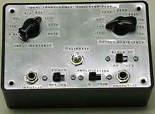
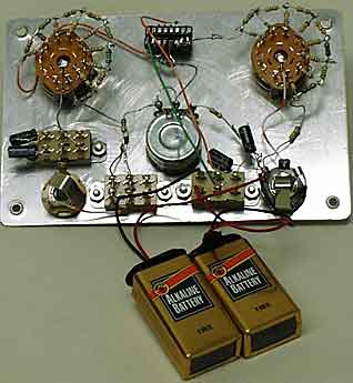
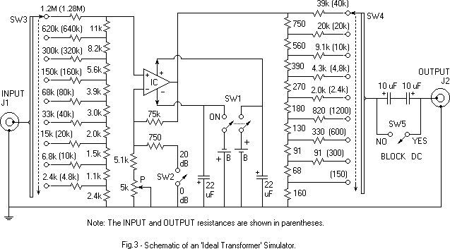
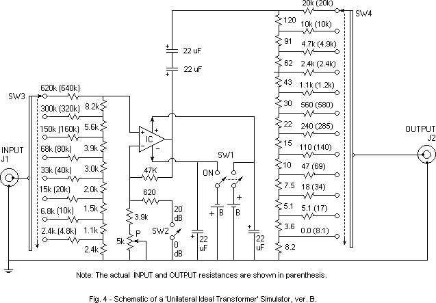
This Article, #15A, used to be Part 1 of the old Article #17. Definitions of terms to be used:
The diode detector circuit to which we will refer is shown in Fig. 1.
Assumptions used in the following discussion:
Approach: The RF signal input power range is divided into two regions and one point; impedance and power relationships are determined. Refer to Figs. 2 and 3. Two Cases will be considered. In Case A, R1=R2=Rxc=0.0256789*n/Is. In Case B, R1=Rxc/sqrt2 and R2=Rxc*sqrt2.
Transition from the linear to the square law region: All good diode detectors, at high input power levels, if well impedance matched at input and output, have a low insertion power loss (a fraction of a dB). If the input power is reduced, at first the output will drop approximately dB for dB in step with the input. If the input is further reduced, the output will start to drop faster (in dB). This can be thought of as the onset of noticeable 'detector insertion power loss'. The insertion power loss at the LSLCP, in two SPICE simulations (see Classes A and B below), is about 5 dB. Put another way, at the LSLCP the output power is about 0.3 times the available input power. This power loss figure changes by less than 0.1 dB between Cases A and B. Most crystal radio sets can deliver a readable signal at an input of Plsc(i) Watts. It would obviously be desirable to lower the input power at which the LSLCP occurs so that more of the weak signals would be closer to the linear mode of operation, experience less insertion power loss and therefore be louder. Example SPICE simulation of a diode detector at 25° C.: Figs. 2 and 3 show power relations at various power levels. The LSLCP is shown by a red arrow. In the SPICE simulations for these graphs, the source and load resistances, R1 and R2, are equal to Rxc (Case A). The DIPL values for Case B (Fig.3) are within 0.4 dB of those of Case A. The main difference is the lower DIPL values in Case B at high input powers. For instance, the insertion power loss at an input of -48.912 dBW is 0.76 dB for Case A and 0.30 for Case B. The loss figures from the equations that follow are quite close to those that occur in a SPICE simulation of both Case A and Case B. At input power levels several times or more below the LSLCP, the impedances of the input and output ports of the detector both approach Rxc for both Cases, A and B. At input power levels several times or more above the LSLCP, the detector approaches operation as a peak detector having a low insertion power loss. In this condition the input RF resistance of the detector approaches half the output load resistance and the output resistance of the detector approaches twice the RF source resistance. Summary: In Case A, the detector input and output ports both approach an impedance matched condition when the signal power is several times lower than that at the LSLCP. At signal power inputs several times greater than that at the LSLCP, a moderate impedance mismatch exists at both the input and output ports. In Case B, conversely, the detector input and output ports are both are moderately impedance mismatched when the signal power is several times lower than that at the LSLCP. At signal power inputs several times greater than that at the LSLCP, both input and output ports approach an impedance matched condition.
Note the following in Fig. 2: At input power levels well above the LSLCP, the relationship between input and output power (see the data points, not the Least Squares Line) approaches linearity. That is, the output changes about one dB for every one dB change in input. At input power levels well below the LSLCP, the relationship between input and output power (see the data points, not the Least Squares Line) approaches a square law relationship. That is, the output power changes about two dB for every one dB change in input power. This has bad implications for weak signal reception. If a weak signal fades, the detected signal will drop twice as many dB as the reduction in input signal strength. For best weak signal sensitivity, one should push the LSLCP to as low a power level as possible. This moves weak signals closer to the LSLCP and linear operation (less detector power loss), and thus increases volume. Lowering of the LSLCP power is associated with using a diode having low values for n and Is, and impedance matching the antenna-ground system impedance and headphone impedance to the now higher values of detector input and output impedances. For good results, one must make sure the impedance transforming means does not introduce other losses. A high Q tank inductor, tuning capacitor, and low loss audio transformer are important. It may be difficult to achieve the required greater impedance transformations in a low loss manner. Example: Assume that Is=38 nA and n=1.03, as was used in the graphs and chart above. Rxc becomes approximately 696009 ohms. R1 and R2 are each fixed at 696009 ohms for all simulation points in Case A. This establishes a very good input and output impedance match at low signal levels and a moderate match at higher levels. The input return loss (S11) is better than -14 dB at signal levels up to 12 dB above Plsc(i). S11 approaches about -9.5 dB at very high input power levels. The input impedance match conditions are reversed in Case B. Rxc is still 696009 ohms but R1 is set to 492153 and R2 to 984305 ohms. Now, at low input power levels, the input and output are somewhat mismatched (S11=-15.3 dB), but at high signal power levels, a very good impedance match is approached. The bottom row shows these two conditions. Unpublished information from Xavier Le Polozec indicates that the optimum practical compromise values for R1 and R2, for input powers well below the LSLCP to well above it is: R1=Rxc and R2=Rxc*sqrt2. The diode detector equations: The following equations are developed for the Class A termination condition of R1=R2=Rxc. They give insertion power loss values to within a fraction of a dB of those provided by SPICE simulation for both Cases A and B. The output current, I2, is different for Class A and B. Observation of a curve of output vs. input power (in dB), from SPICE simulation of a Class A terminated detector reveals a slope of 1.5 at an input power value of -78.91 dBW, for the particular diode used. This is the LSLCP for input power. Another observation is that the rectified diode current I2 at the LSLCP point appears to be very closely two times the Is of the diode. This two times figure appears to be apply to all diodes. Note: The Plsc(i) of -78.91 dBW occurs when the detector parameters are R1=R2=Rxc and the diode parameters are: Is=38 nA, n=1.03 and temperature is 25° C. In general, the 'two times' figure does not hold for termination conditions other than R1=R2=Rxc. Differentiating the Shockley diode equation with respect to the diode junction voltage yields. Diode junction resistance=Rxc=0.0256789*n/Is ohms. (0) I2=2*Is. (From the paragraph above) (1) Some obvious relations: Output power=Po=(I2^2)*R2
Watts. The output load R2 has been specified as equal to Rxc, Rxc is
defined in equation (0) and I2=2*Is at the LSLCP. Substituting into the
equation for Po, we get: A proper relation between Po, Pi and I2 requires that I2 approach zero as Po/Pi approaches zero, that Po/Pi approach proportionality to I2 as I2 becomes low (the square law relation) and that Po approach Pi as I2 becomes very high. Also, at an output power of Plsc(o), I2 must equal 2*Is. Curve fitting suggests this relationship: Po/Pi=(I2/(I2+4*Is). This equates to: DIPLR=I2/(I2+4*Is) (3) Since, at the LSLCP, I2=2*Is (eq. 1), Plsc(i)=Plsc(o)*3. (4) Substituting the value of Plsc(o) from equation 2 into equation 4 results in: Plsc(i)=0.308148*Is*n (4a) A lot of mathematical manipulation of the relations given above results an equation that fits the simulation data quite well over the whole range of the graph in Fig. 2. Po=[sqrt(0.102716*n*Is+Pi)-sqrt(0.102716*n*Is)]^2 Watts. (5) Po={sqrt[Plsc(o)+Pi]-sqrt[Plsc(o)]}^2 Watts. Normalized to Plsc(o). (5n) A rearrangement of the terms in equation (5) yields: Pi=Po+sqrt(0.41104*n*Is*Po) Watts. (5r) Pi=Po+2*sqrt(Plsc(o)*Po) Watts. Equation (5r) normalized to Plsc(o), by using equation (2). (5rn) From equation (5r), at low output power power levels, the input power required to produce a given output approaches: Pi=sqrt(0.41104*n*Is*Po) (5Li) Prearranging terms of equation 5Li: Po=(Pi^2)/(0.41104*n*Is) (5Lo) An equation that fits the detector insertion power loss ratio (DIPLR) is obtained by dividing equation (5) by Pi: DIPLR=[sqrt(1+0.102716*n*Is/Pi)-sqrt(0.102716*n*Is/Pi)]^2 Ratio of output to input power (Po/Pi). (6) DIPLR={sqrt[1+Plsc(o)/Pi]-sqrt[Plsc(o)/Pi]}^2 Normalized to Plsc(o) by dividing eq. (5n). (6n) One can determine the DIPLR at which the diode detector is operating, for a particular signal being received, assuming that the phones are reasonably well impedance matched to the output resistance of the diode. Adjust the DC load on the detector to 0.0256789*n/Is ohms.** Measure the DC voltage V2 developed across the DC load resistor. DIPLR=V2/(V2+0.1027156*n) (7) Interesting note: A simple manipulation of Equations #0, 2 and 4 shows that, at the LSLCP, the RMS value of the AC signal at the input of the diode is: (0.08895*n) V, and it is independent of Is. ** See articles #16 and #27 for info on determining the Is and n of diodes as well as measurements on some diodes. Equation (5r) seems important. It shows that the input power required for a specific output power is reduced if n and/or Is is reduced. At low input powers, the required input power for a specific output power approaches direct proportionality to the square root of n and/or Is, as shown in equation (5Li). The product n*Is can be considered to be a 'figure of merit' for diodes as weak signal detectors, provided input and output impedance matching exist and lossesw from passive components remain unchanged. The ideality factor (n) and saturation current (Is) of the diode are important parameters in determining ultimate very weak signal sensitivity. If all other diode parameters are kept the same, the weak signal input and output resistances of a diode detector are directly proportional to n and inversely proportional to Is. Assume a diode with a value of n equal to oldn is replaced with an identical diode, except that it has an n of newn, and the input and output impedances are re-matched (the new impedances are doubled). The result will be a detector insertion power loss change of: 10*log(oldn/newn) dB. That is, a doubling of n will result in a 3 dB increase in insertion power loss, assuming the input power is kept the same and input and output impedances are re-matched. The result is a 3 dB reduction of output power (volume). A similar effect occurs if Is of the diode is increased except that this change reduces the impedances that must be rematched instead of increasing them. Warning: Don't use two diodes in series if you want the best weak signal sensitivity. The result of using two identical diodes in series is the emulation of an equivalent single diode having the same Is but an n of twice that of one original diode. Experimental measurements on eleven different diodes used as detectors is shown in Article #27. Close correlation between these equations and actual measurements is demonstrated. |

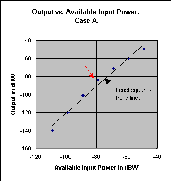
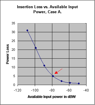
|
A Procedure for Measuring the
Saturation Quick Summary: A schematic and operational instructions are given for a device for use in measuring Saturation Current and Ideality Factor of a diode. Measurements of various detector diodes are included. The Saturation Current and Ideality Coefficient of a diode can be determined by measuring an applied junction voltage along with the associated current flow at two different voltages. These two data pairs are then substituted into the Shockley diode equation to create two simultaneous equations in Is and n, and then solved for Is and n. Since the equations include exponential functions, they can not be solved by ordinary algebra. Numerical methods must be used. The Shockley diode equation at 25 degrees C. is: Id = Is*(exp(Vd/(0.0256789*n))-1) Amps. Id = Diode Current (amps), Is=Saturation Current (amps), Vd = Diode Voltage, n = Ideality Coefficient. The series resistance Rs of the diode is ignored because the measurement currents are so low that the voltage drop across Rs is negligible. Measurements have shown that Is and n of point contact germanium diodes can vary with current, but are relatively constant, down to very low currents, when the current is under six times Is. Silicon p-n junction diodes exhibit values of Is and n that vary with current. The values for Is and n of Schottky diodes are quite constant over the range of currents used in ordinary crystal radio set reception. A convenient set of measuring currents is about 6*Is and 3*Is. Substituting Id = 6*Is, then Id = 3*Is into the Shockley and solving for Vd yields: For Id = 6*Is, Vd = 0.05000*n volts. For Id = 3*Is, Vd = 0.03561*n volts. The value of n will probably be between 1.0 and 1.2 for the type of diodes used in crystal radio sets, so use 1.1 in determining the applied voltage to use. Suggested voltages to use are about 0.055 and 0.039 volts, although other values may be used.
S1 is a triple pole double throw switch, S2 is a push button momentary-contact SPST switch. DVM is a digital voltmeter with 10 Meg input resistance having a 200 mV range setting. S3 is a range switch that enables greater precision when using a conventional 3 1/2 digit DVM. It is also used when measuring diodes having a high Is. R2 is used for coarse setting of the diode voltage. R1 is a ten turn precision 20k pot such as part # 594-53611203 from Mouser. It is used for fine setting of the diode voltage. Procedure for Measuring Is and n:
There is currently available on the Web, a program from Polymath Software at: http://www.polymath-software.com/. This program has many capabilities, and among them is a nonlinear equation solving capability. A free demo copy of the latest program is available for download, but is limited to 20 uses. After that, for more usage, you have to buy it. Some programmable pocket calculators include a nonlinear equation solver. One calculator that has one is the HP 32S Scientific Calculator. A program to solve for n and Is takes only 28 steps of program memory and is here. Mike Tuggle posted on 'The Crystal Set Radio Club' the following simple procedure for determining Is and n by using a spreadsheet. "In lieu of an equation solver package, the Schottky parameters can be solved for by simple trial-and-error. This is easily done with an ordinary spreadsheet, like Excel or Lotus. For the two measurement points, (Id1, Vd1) and (Id2, Vd2), set up the spreadsheet to calculate: Id2[exp(Vd1/0.0257n) - 1] and, Id1[exp(Vd2/0.0257n) - 1]. Then experimentally plug in different trial values of n, until the two expressions become equal. This gives the correct value of n. Now, plug this value of n into: Is = Id1 / [exp(Vd1/0.0257n) - 1] or, Is = Id2 / [exp(Vd2/0.0257n) - 1] to get the correct value of Is." An Excel spreadsheet constructed as Mike suggested is here. An example from data taken on an Agilent HBAT-5400 is entered, for reference, on line 2. Line 3 may be used for calculations using data from other diodes. Column H automatically calculates a value for Is each time n is changed. All one has to do is enter the values as described above in columns A through E and hit enter. Caution: If one
uses a DVM to measure the forward voltage of a diode having a high
saturation current, a problem may occur. If the internal resistance of
the DC source supplying the current is too high, a version of the
sampling voltage waveform used in the DVM may appear at its terminals
and be rectified by the diode, thus causing a false reading. One can
easily check for this condition by reducing the DC source voltage to
zero, thus leaving only the internal resistance of the source in
parallel with the diode, connected across the terminals of the DVM. If
the DVM reads more than a tenth of a millivolt or so, the problem may be
said to exist. It can usually be corrected by bypassing the diode with
a ceramic capacitor of between 1 and 5 nF, preferably, an NPO type. I
use a 0.047 uF NPO multi-layer ceramic cap from Mouser Electronics.
Connect the capacitor across the diode with very short leads, or this
fix may not work. Tips
Note: A simplified method of determining the Saturation Current of a diode, if the Ideality Factor is estimated in advance is shown in Section #2 of Article #4. Summary of measurements on some diodes: The following charts show typical values for Is and n for diodes that might be used in crystal radio sets. One can see, for any particular diode, that Is and n do not vary by much over a moderate current range. Therefore, they may be considered to be dynamically constant when receiving a signal. Each value of n and Is is calculated from two voltage/current pairs as described above. The diode current (Id) given for each of the n, Is pairs is the geometric mean of the two currents used in the measurement. A Fluke model '89 IV' 4-1/2 digit DVM was used to enable measurements down to as low as 15 nA on some diodes. Noise problems cause some measurement error at low currents. That is the reason for the fluctuations in some of the readings. Values of n very close to 1.0 or below are obvious measurement errors. Those low values for n should have come out somewhat higher and the associated values of Is, also higher. Note that the germanium diodes show an unexpected tendency to increased values for Is and n at the higher currents. The 1N4148 silicon p-n junction shows the expected increase of Is and n at lower currents. The Schottky diodes seem to have pretty constant values of Is and n across the current ranges measured. Experiments described in Article #27 indicate that the measured values of Is and n for silicon Schottky diodes tested here, when used as detectors, remain at the measured values at rectified currents so low that a voice signal is barely readable. This is not necessarily true for all germanium diodes.
* This Infineon diode has an unusually high series resistance of 130 ohms. The voltage drop across this resistance is low enough in all the measurements to be ignored, except for the highest current one. There, a correction for the voltage drop was made.
A rare germanium diode that seems to be ideal for many crystal radio set designs is the FO 215, branded ITT. A search of the Internet has not turned up a manufacturer's datasheet. ITT is not in the germanium diode business anymore, but from the Internet search it appears that the original company was a German company named ITT Intermetall. Some of their semiconductor business became ITT Semiconductors. This was later sold, around 1997 to General Semiconductor Industries. That business was later sold to Vishay. One source indicated that General Instruments was also one of the intermediate owners. Averages of measurements on three samples of the FO 215 are: Is=109 nA and n=1.02. These measurements were made at an average current of about 250 nA. Interesting note: The average Is of the FO 215 diodes is about equal to the geometric mean of that of the Agilent 5082-2835 and a typical 1N34A. I obtained my FO 215 diodes from Mike Peebles at: http://www.peeblesoriginals.com/ . Article #27 shows detector measurements of how diodes having different values of Is and n perform as weak signal detectors when impedance matched at both input and out put. |
|||||||||||||||||||||||||||||||||||||||||||||||||||||||||||||||||||||||||||||||||||||||||||||||||||||||||||||||||||||||||||||||||||||||||||||||||||||||||||||||||||||||||||||||||||||||||||||||||||||||||||||||||||||||||||||||||||||||||||||||||||||||||||||||||||||||||||||||||||||||||||||||||||||||||||||||||||||||||||||||||||||||||||||||||||||||||||||||||||||||||||||||||||||||||||||||||||||||||||||||||||||||||||||||||||||||||||||||||||||||||||||||||||||||||||||||||||||||||||||||||||||||||||||||||||||||||||||||||||||||||||||||||||||||||||||||||||||||||||||||||||||||||||||||||||||||||||||||||||||||||||||||||||||||
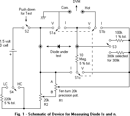
|
New ways to Increase Diode Detector Sensitivity to Weak Signals, and a way to determine if a diode detector is operating above or below its Linear-to-Square-Law Crossover Point Quick Summary: The very low signal sensitivity of a crystal radio set can be improved by cooling the diode. This possibility arises when the rectified DC current is below about twice the Saturation Current of the diode. Also see Article #28 for more info on increasing weak-signal sensitivity. Definitions of terms to be used:
The old Article #17 has been separated into two Articles. This new Article #17A is a revision of Part 2 of the old #17. Part 1 has been broken out and renamed "Quantitative Insights into Diode Detector Operation Derived from Simulation in SPICE, and some Interesting new Equations.". It is numbered15A. Assume that a station one can barely read has a power sufficient only to operate the detector at or below the "Linear-to-square law crossover point" (LSLCP). This is the point where the rectified diode DC current is about twice Is. Volume can be increased if the Plsc(i) point could be shifted to a lower RF power level. This will result in less insertion power loss since operation will now be closer to the linear region. The RF power required to operate a diode detector at its Plsc(i) point (at 25° C.) is shown as equation (4a) in Article #15A. It can be rewritten as: Plsc(i)=0.0010341*Kt*Is*n Watts (1) When referring to the schematic of a diode detector, Figure 1 will be used.
Fig. 1 Diode Detector Output and Insertion
Loss vs. Input Power. The LSLCP
It is assumed that input and output are impedance matched. One can see from equation (1) that if Is, Kt or n can be lowered, the Plsc(i) point is lowered and therefore, the volume from weak signals can be increased. The reciprocal of the product of Is, n and Kt can be seen to be a sort of "weak signal diode figure of merit" (WSDFM). It has been shown that in all semiconductor diodes, a small % drop in Kt will result in a much larger % drop in Is from its initial value. It must be remembered that the reduction of Is or Kt increases Ri and Ro. If n is reduced, Ri and Ro are reduced. Re-matching of impedances (Ri and Ro) is required to gain the benefits being sought.
The ideality factor (n) of the diode is an important parameter in determining very weak signal sensitivity. If all other diode parameters are kept the same, the weak signal input and output resistances of a diode detector are directly proportional to the value of n. Assume a diode with a value of n equal to oldn is replaced with an identical diode, except that it has an n of newn, and the input and output impedances are re-matched. The result will be a detector insertion power loss change (weak signals only) of: 10*log(oldn/newn) dB. That is, a doubling of n will result in a 3 dB increase in insertion power loss, assuming the input power is kept the same. This illustration shows the importance of a low value for n. Warning: Don't use two diodes in series if you want the best weak signal sensitivity. The result of using two identical diodes in series is the simulation of an equivalent single diode having the same Is but an n of twice that of one original diode. A diode detector is operating at its LSLCP (usually with about a 5 dB insertion power loss), if the average rectified DC voltage across the resistive component of its load is (n*51) mV. (If one doesn't know the n of one's diode detector, it can usually be assumed to be about 1.07). A requirement for the (n*51) mV relation to be correct is that the detector be approximately impedance matched at its input for RF and at its output for audio and DC. Specifically, the DC load resistance must be set to 0.026*n/Is ohms (see Part 4 of Article #0 for info on n and Is). See Fig. 5 in Article #26 for a method of adjusting the DC resistance of the diode load and monitoring the rectified voltage. Typical values for n and Is for many diodes may be found in Articles #16 and 27. The audio load AC impedance matching requirement is not absolute if one is interested only in hearing the volume delivered from ones headphones when the diode is operating at its LSLCP. The reason is that volume is a slow and gradual function of audio mismatch, for moderate mismatches. A two-to-one audio mismatch causes a loss in audio output of only 0.5 dB. A four-to-one mismatch causes a loss of 1.9 dB (hardly audible). |

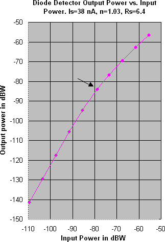
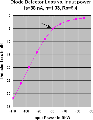
One third the total power in a 100% modulated AM
signal is in the sidebands that carry the audio modulation. An
ideal, 100% efficient Crystal radio set will convert all of the received
sideband power to audio output power. Call it audio power output #1.
What about the other two thirds of the power? That is the power
in the AM carrier that carries no audio information but has twice
the power of the sidebands (at 100% modulation). This Article shows the
circuit of a device that can be used to extract that carrier power and
use it to operate a micro-power op-amp. The op-amp uses the detected
audio voltage from the diode detector for its input and provides an
additional source of audio power. Call it audio power output #2. These
two audio power sources, #1 and #2 can be added together to create a
final output at least 3 dB more than the normally available audio power
output #1. 1. Background Within the last year or so, Burr-Brown (now owned by
Texas Instruments) came out with a micro-power op-amp (OPA349) specified
to work with as little as a 1.8 volt DC power source. It draws a
minuscule 1 uA quiescent supply current. This op-amp opens the
possibility of building a device I call a "Free 3 dB Detector Load" (F3dBDL).
I have found that the F3dBDL will actually operate with an input signal
low enough to generate a rectified voltage as low as 1.2 volts DC.
Maybe all the OPA349s will work in this circuit at 1.2 volts. My F3dBDL
requires a minimum input carrier power of -53 dBW and a rectified DC
voltage of at least 1.2 volts. 2. A conventional diode detector with standard output loads (DC and audio) Any crystal radio set that uses an audio output
transformer can be represented by the simple circuit shown in Fig. 1.
V1, R1 represent the antenna-ground power source, impedance transformed
to the tank circuit. The detected carrier power is dissipated in the
resistive load R2. The detected side-band power is delivered to the
audio load R3.
3. Conventional crystal radio set detector with the F3dBDL The F3dBDL is intended to be used with signals strong
enough to cause the detector to operate in its peak-detection mode. In
this case, the DC load R2, seen by the diode D1 should equal to two
times the RF source resistance R1. D1 should also see an AC load
resistance of two times R1, at the primary of transformer T1. (See
Article #0 , Section 4, for more info on this.) The power dissipated in
the DC load R2 in the circuit in Fig. 1 will be used, in Fig. 2, to
power the op-amp U1. In Fig, 1 the audio output power is delivered to
the output load R3. In Fig. 2 audio output power is delivered to two
loads of value R3 and k*(R3). With proper selection of the relative
impedance transformation ratios of T1 and T2, the value of k may be
made equal to about 1. In addition, the output currents of T1 and
T2 become about equal. In this case, no current will flow in connection
X, and it can be eliminated. This gives us one 600 ohm instead
of two 300 ohm outputs. The resultant load resistance of twice
R3 will absorb twice the audio power than did R3 in Fig. 1, although at
twice the impedance (600 ohms). The resistive network R4, R5, R6 and
R7 biases + input terminal of U1 at 1/2 the DC supply voltage appearing
across C2 and attenuates the detected audio voltage appearing across C1
so that it will not overload U1. The value of capacitor C2 is made
quite large to enable it to hold steady the voltage it supplies U1,
between bursts of speech.
If all the power in the carrier could be changed to audio power and added to the main detector audio output, the total audio power would be tripled, a 4.8 dB increase. It would be nice if the op-amp had 100% efficiency in converting its input DC power to output audio power, but it doesn't. An ideal class B amplifier has a theoretical efficiency of 78.5%. Therefore, we lose at least 21.5% (1.05 dB) right off the bat. Other losses in the op-amp, the 1 uA quiescent current of the U1 and the bias network R5, R6 and R7 use up some more of the 4.8 dB. The transformer T1 has losses and uses up some more of the 4.3 dB. We are left with an output power from the U1, T2 combination about equal to that of a conventional crystal radio set. The two added together gives the 3 dB increase. There are some limitations in using the F3dBDL. The IC is specified to operate over a supply voltage range of 1.8 to 5.5 volts. In this circuit it seems to work well over a supply voltage range of 1.2 to greater than 5.5 volts. This corresponds to an input carrier power range of -53 to >-40 dBW. I have found, that for me, the volume to be too great for headphone use but barely adequate for high efficiency horn speaker use. If more than -40 dBW of AM signal carrier power is available, the F3dBDL can be made to handle it (and give a greater sound volume) if the F3dBDL is operated at a lower output impedance level. In this case, transformers T1 and T2 might have to be changed to ones with a lower transformation ratio. The impedance at the + signal input terminal of U1 is very high. Use care to minimize stray capacitance to ground at this point. Too much will roll off the highs. The high audio frequency output capability of U1 falls as signal strength and, as a result, supply voltage increases. This can cause audio distortion. The F3dBDL can also be used to increase the volume on weak stations. This is done by connecting a ceramic electric double layer high capacitance capacitor across C2, charging it up overnight on a strong station and then switching it to power the opamp for weak station listening later on. A 0.047 Farad capacitor will hold its charge for many hours in this application. One manufacturer of this type capacitor is Panasonic, and one of their distributors is Digi-Key Corp. If the load on the F3dBDL is a SP headphone set with the elements wired in series, bass response can be improved with a small subjective increase in volume. Consider the two headphone elements as the two impedance equal loads R3 and k*(R3), in Fig. 2. Restore the connection X. The element k*(R3) will have a much better bass response than the other one because it is driven by the low output resistance of the opamp. See "It is interesting to note" at the end of Section 1 in Article #2 for more info on this. Last, but not least, one should not expect too much from the F3dBDL. After all, a 3 dB or so increase in volume will not be perceived as a lot. The challenge of this project was to devise a way to use all of the power in an AM modulated signal, I believe that has been accomplished. |
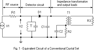
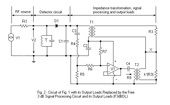
Two assumptions made in the analysis: They are that the distributed capacity between the two coil windings may be represented by one lumped capacitor, Cc, connected between the center of one winding to the center of the other. See Fig. B. The other is that the magnetic coupling between the primary and secondary windings is very high. This assumption is close to reality for the bifilar wound portion of the transformer, provided the capacity coupling is not too high. The magnetic coupling between the bifilar-ed parts and the end windings is not as close as that between the bifilar-ed parts. This does not affect the validity of the analysis. Keep in mind that in transformers with unity coupling, the ratio of the voltage on any winding to any other is directly proportional to the number of turns on each winding. This also applies to a portion of one winding. (Just use the number of turns in that portion.) Figures A through E show the inductive circuit through various changes as the following reduction and simplification proceeds. Simplification and reduction of the circuit of the Mystery crystal set using the "Broad" non-earthy antenna connection: The physical circuit of the Mystery set is shown in Fig. 1 with the antenna connected to the non-earthy side of the primary. The dots on the windings show the start of each winding, assuming that they are both wound in the same direction. Figure 2 shows a coupling capacitor Cc, between the two windings. It represents the parallel combination of two distributed capacitances: One is formed of the dielectric of the wire insulation between the bifilar-ed primary and secondary coil turns. The other is also between the primary and secondary coil turns, but in this case, there are three dielectrics in series. They are: (1) The dielectric of the insulation on, say, the primary winding that is in contact with the coil form. (2) The dielectric of the coil form between the primary and secondary windings. (3) The dielectric of the insulation on the secondary winding that is in contact with the coil form. Cc is in a series circuit with the antenna and ground. Fig. 3 shows Cc shifted up to the antenna and out of the way. No change in performance will result. The top and bottom leads of the secondary are connected (each 12.5 turns from the center), to the corresponding points on the primary (12.5 turns up and down from the center). This is shown in Fig. 4. Since the points that are connected together have the same AC voltage on them, no current will flow through their connection and the circuit operation will be undisturbed. Figure 5 shows the resulting equivalent circuit from the connections made in #4.. Since all portions of the winding are assumed to be unity-coupled to each other, performance will not change if the tuning capacitor C1 is connected as shown in Fig. 6, as long as its value is changed appropriately. C1 is connected across 50 turns of the inductor. C2 is connected across 37.5 turns. The inductances of a unity coupled 1:1 transformer are directly proportional to the square of the number of turns. The number of turns across which C2 is connected is 3/4 of the number of turns turns across which C1 is connected, therefore, the inductance across which C2 is connected will be 9/16 the inductance across which C1 is connected. C2 must be increased from the the value of C1 to 16/9 of C1 for the circuit to work the same as before the transformation. The bottom portion of the coil in Fig. 6 can be eliminated since nothing is connected to it. The final result is the equivalent circuit shown in Fig. 7. Here we see a conventional crystal set circuit with the antenna-ground components connected directly across the full tank, with isolation from full antenna resistive loading supplied by the capacitor Cc. The detector load is tapped in at 2/3 of the tank voltage to reduce its resistive loading effect on the tuned circuit. That's it for the non-earthy "Broad" antenna connection. Simplification and reduction of the circuit of the Mystery crystal set using the "Selective" earthy connection. Figures 8 through 14 show the simplification and reduction of this circuit. It proceeds in an manner similar to the one for the "Broad" connection. Now look at Fig. 14. The value of Cc is unchanged from that in Fig. 7. C3 will have to be somewhat larger than C2 was for the circuit to work the same. The antenna-ground components and Cc are now connected across only 1/3 of the tank instead of the full tank. The detector load is still tapped in at 2/3 of the tank voltage. That's it for the earthy "Selective" antenna connection. What might the value of the magnetic coupling coefficient between the bifilar-ed portion of the windings be? To think about this, consider: Mentally unwind the bifilar portion of the coil from the coil form, but imagine the two wires are still in the same relative positions to each other. Stretch them out. The ends of one wire are the terminals of one winding of a transformer and the ends of the other winding, the terminals of the other. Now you have two parallel wires closely spaced and several tens of feet long. The spacing (from the wire insulation) between them is maybe 0.005". It should seem obvious that the magnetic coupling between them could not get much greater (without ferrite cores), no matter what one does with the wires. It can, however become greater when the bifilar wire is wound on a form. The reason is that places a primary wire on each side of every secondary wire and vice-versa, providing more magnetic coupling between the windings than when the wires are stretched out. Here is an approach for determining the coupling coefficient of a bifilar winding: Construct a bifilar wound coil that has about the same inductance as the bifilar-ed wires in a standard Mystery" set. This inductance calculates out to be 57 uH. No wire of the gage originally used was available, so the largest bonded bifilar wire I had available was used. It was made by MWS Wire and consisted of two #30 ga. film insulated wires bonded together. Its cross section measures 0.012x0.024". Twenty turns were wound on an available 3 1/2" styrene coil form since a 3" diameter coil form, as used in the original Mystery set was not available. The winding length came out to be a very small 0.475" because of the small wire size. This is much less than that in the original Mystery set but, tough, that wire is all that was available. The leads from the coil were still bifilar-ed, 10" long ends. Several resonance measurements were then taken using a Q meter. The first was with one winding connected to the inductance terminals of the Q meter, the other winding being open circuited (Loc), at several frequencies from 0.515 to 2.36 MHz. The indicated capacitance readings on the Q meter were noted. The other was with the same winding still connected to the inductance terminals of the Q meter but with the other winding shorted (Lsc), at frequencies from 3.0 to 11.0 MHz. Again, the indicated Q meter capacitance readings were noted. At frequency extremes these readings will be distorted by the presence of distributed capacitance between the two windings, 1020 pF in this case. The conventional Mystery set would have considerably less capacitance between the windings because of the much thicker insulation on the wires. Note: The capacitance between the windings cannot be determined at RF by the use of a Q meter. It can be measured by the use of an RLC bridge operating at 1 kHz or a DVM having a capacitance measuring function (if it operates at about 1 kHz). Over the frequency range of 0.515 to 1.71 MHz, Loc was calculated to be: 66.5 +/- 2.5 uH. Over the frequency range of 3 to 7 MHz, Lsc was calculated at: 2.01 +/- 0.06 uH. A derivation results in the following relation for the coupling coefficient between two identical magnetically coupled inductors: k=sqrt(1-Lsc/Loc). The calculated coupling coefficient between the two bifilar-ed windings is 0.984, which I consider very close to unity. The bifilar wire was re-wound on the same form, but spaced to cover a 1" length. The coupling coefficient came out at 0.966 and the distributed capacitance: 895 pF. Another coil was then wound from the same piece of wire on a 1.5" diameter polypropylene form. The winding was slightly space wound and had a length of 1.5 ". Coupling coefficient: 0.983 and distributed capacity coupling: 945 pF. Of course, manufactured, bonded, bifilar wire is not recommended for use in a Mystery set. Usually two independent, insulated wires are wound close spaced. This practical case results in substantially less distributed capacitance than when using bonded wires. Conclusion: The beauty if the Mystery set is that it provides an antenna decoupling capacitor (Cc) (made from the distributed capacity between the bifilar-ed windings), along with the effect of two different points for its connection to the tank; all without any specific physical capacitor or taps on the inductor. Further, the diode is effectively tapped 1/3 down on the tank for improved selectivity. The only downside to this arrangement is some loss caused by the probable relatively low Q of Cc. When using the "Broad" antenna connection, the antenna-ground components are connected through Cc across the full tank. This arrangement puts a relatively large amount of antenna resistive loading on the tank. The loading results in as reduced selectivity, but stronger signal strength than one gets in the "Selective position. See Fig. 7. When using the "Selective" antenna connection, the antenna-ground components are connected through Cc across only 1/3 of the tank coil turns. This results in a reduction to about 1/9 of the resistive loading by the antenna on the tank, compared to the loading in the "Broad" connection. See Fig. 14. This reduced loading increases the loaded circuit Q, and hence selectivity. The ratio of unloaded to loaded Q is reduced, thus reducing sensitivity. For practical purposes the 'leakage inductance' between that part of the primary that is bifilar wound with the secondary is very low. To the extent that it is not zero, it and the leakage inductance between the outer turns of the primary and the inner bifilar-ed 25 turns can be considered to be an added "leakage inductance" in series with C2 in Fig. 7; and in series with C3 in Fig. 14. The main effect of this leakage inductance, compared to having none, is to somewhat lower the highest frequency than can be tuned. The low end of the tuning range will be extended a small amount. |
Quick Summary: This
Article describes a method to measure the series capacitive and
resistive parameters of the impedance of an antenna-ground system vs
frequency. Results from measurements on an attic antenna are given.
The circuit in Fig. 1 was inspired by an Article in The Crystal Set Society Newsletter of Jan 1, 1995. It was written by Edward Richley. He used a 1 MHz crystal oscillator for his source, so had no problem with using a 200 uA meter. I use a sine wave function generator for my RF source, but a radio Service man's oscillator may also be used if it has enough output. Either of these sources cannot supply as much signal as the xtal oscillator, so I had to increase sensitivity. That's what the 2.5 mH chokes and 5 nF caps are for. The 2.5 mH chokes eliminate RF loading by any resistive component of the meter or phones on the diode detector. The 5 nF caps eliminate resistive DC loading on the detector from the two 680 ohm resistors. I lay out the components breadboard style on a nonconductive table to minimize stray capacity, keep connections short, and especially keep the signal source lead of J1 away from the connections to each end of D1. In my setup D1 is a 1N34A, M1 is a 0-20 uA DC meter, R1 is a 75 ohm non-inductive carbon pot and C1 is a two gang variable cap of 365 pF per section. I parallel the two sections when the antenna capacitance is above 365 pF. A lower sensitivity meter can be used than the one used here, at the cost of a requiring a higher applied signal to J1. If a sensitive enough meter is not available, a pair of high impedance phones (2000 ohms DC resistance) or preferably, a sound powered pair with the elements wired in series can be used. In this case, the generator must have its AM audio modulation turned on at its highest level. A modulation frequency of about 1 kHz is recommended. If the meter is used, do not connect the phones. If phones are used, do not connect a meter. To use the bridge, tune the generator to a frequency of interest. Adjust C1 and R1 for minimum deflection on M1 or a null of the modulation tone in the phones. Increase the RF signal to J1 as much as possible in order to get the sharpest and most precise null. Measure the resistance of R1 with an ohmmeter. Use any desired method to measure C1. I use the cap. measurement range of my Fluke DVM. I'm sure the reader does not need to be reminded that this test involves radiating a weak RF signal from the antenna when making the measurements, so the length of time the generator is on should be kept as short as possible. Possible issues: More sensitivity is needed or interference from antenna pickup of local stations obscures the bridge null. If insufficient signal is available from the RF generator to provide satisfactory meter readings, one can use the more sensitive broadband circuit shown in Fig. 2. The values of L1 and L2 are 2.5 mH and C2 is set to zero in the broadband version. A full wave rectifier is used instead of the half wave one used in Fig.1 and it gives about twice the output. One can also change from using 1N34A diodes and try Schottky Zero Bias detector diodes such as the Agilent HSMS-2850 in either circuit. The HSMS-2855 Zero Bias diode is especially suitable for use in the circuit shown in Fig. 2 since it is a package having two independent diodes, one for D1 and the other for D2. One must be cautious when using the HSMS-2855 because the diodes can be damaged by the application of too strong a signal to J1. This can happen if the signal generator signal is very strong when the bridge is greatly unbalanced. It's best to start with a weak signal, balance the bridge, then increase the signal if necessary. If the signal from the RF generator is not strong enough to override local pickup, thus obscuring the meter null, selectivity may be added to the bridge shown in Fig. 2 by making use of C2 and changing L1 and L2. If L1 and L2 are changed to, say, 10 uH inductors and C2 is made equal to 1200 pF, the bridge will be tuned to about 1 MHz. These changes will reduce the influence of local pickup upon measurement of antenna-ground impedance at 1 MHz. One suitable 10 uH inductor is Mouser's "Fastron" #434-23-100. If one uses headphones instead of a meter as the null indicator, even greater sensitivity can be achieved by AF modulating the bridge signal generator and connecting a parallel L/C tuned to the modulating frequency of the generator across the phones. This will filter out much of the interfering cross talk from local pickup and pass the modulation tone with little loss. Suggested values are L=47 mH and C=0.5 uF if the modulating frequency used is about 1 kHz. A low cost coil having an inductance of 47 mH and a Q of about 9 at 1 kHz is available from Mouser as a Fastron Plugable Shielded coil, #434-02-473J ($1.20 each). Greater selectivity against cross-talk can be obtained by decreasing the inductance and increasing the capacitor. I live about 9 miles from WOR and 12 from WABC, both 50 kW stations. 10 volts peak-to peak applied to the bridge overrides the local radio station pickup sufficiently to provide a clear null on the meter when using the circuit shown in Fig. 1 when using a 1N34A diode. A useable null with an applied signal of only 1.5 volts p-p can be obtained when using the circuit in Fig. 2 with zero bias detector diodes, sound-powered phones instead of a meter and the parallel LC filter. Notes:
What can one do with the measurement results? The main practical thing one can do with the bridge is to Measure and Monitor antenna-ground circuit resistance. This resistance comes primarily from the physical ground, not the antenna and ground connecting leads or radiation resistance of the antenna. Any increase in the antenna-ground resistance serves to reduce the signal power available from the antenna. Any decrease, of course increases it. A halving of the antenna-ground system resistance provides a 3 dB increase in available signal power, if one properly rematches to the crystal radio set input circuit. Measure: One can experiment with different
grounds and various ground paralleling schemes to come up with the one
that has the lowest resistance. Use of this one will result in
maximizing the available signal power (more volume). Experiments using
a counterpoise ground can be made. The other thing one can do, if one is
mathematically engineering a crystal radio set, is to use the R and C
values as parameters in the design. See Article #22. Measurement results on an indoor
attic antenna system: The measured antenna-ground system capacitance was 295 pF at 0.5 MHz, 325 at 1.0 MHz, 410 at 1.5 MHz and and 660 at 2.0 MHz initially. The respective series resistances measured: 17, 12, 10 and 14 ohms. The equivalent reactance elements of this antenna are a capacitance of 285 pF in series with an inductance of 12.5 uH. Since my ground is composed of the house cold water supply pipes in parallel with the the hot water baseboard heating system pipes, much of the capacitance from the horizontal attic antenna wire is to them and the roof, not a real resistive earth ground. That, I think explains the low resistance and high capacitance readings. Probably the ground system is acting as a sort of counterpoise. I decided to see if I could get greater signal pickup by changing to a very crude simulation of a flattop antenna. To do this, I paralleled the antenna wire with a piece of TV twinlead connected to it at each end and at the point of down-lead takeoff. The twinlead was separated from the 7/26 wire by about 2 1/2 feet. The new measured antenna-ground system parameters became: Capacitance: 430 pF at 0.5 MHz, 510 at 1.0 MHz and 860 at 1.5 MHz. The respective series resistance values became: 15, 12 and 11 ohms. The equivalent reactance elements became a capacitance of 405 pF in series with an inductance of 14.2 uH. Signal pickup increased by a negligible 0.8 dB at 710 kHz, and even that was, I'm sure, within experimental error. One may want to compare these equivalent impedance components with the 'Standard Dummy Antenna', as specified in 1938 by the IRE (Institute of Radio Engineers) in 'Standards on Radio Receivers'. My reference for this is Terman's Radio Engineer's Handbook, first edition, 1943, pp 973 and 974. A rather complex equivalent circuit for the antenna is shown on page 974. It is stated that a simpler alternative network, given in footnote #2 on page 973, can be used when only the BC band is of interest. It consists of the series combination of a 200 pF capacitor, 25 ohm resistor and 20 uH inductor. Terman states that the two antenna equivalent circuits have closely the same impedance characteristics in the BC band. The impedance graph on page 974 and the impedance from the series combination of 200 pF, 25 ohm resistor and 20 uH differ, particularly in the resistive curve in the complex equivalent circuit. The 25 ohm resistance in the simplified circuit is probably taken from the resistance in the complex circuit, at the geometric center of the BC band. This resistance is shown as constant in the simplified circuit, and as a strong function of frequency in the more complex circuit. It is suggested that the complex equivalent circuit is theoretically derived, assuming a perfect ground and therefore does not include the resistance of the ground return path. The ground circuit can easily add 15-50 or more ohms to the circuit. |
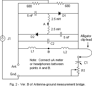
|
Design, construction and measurement of a single-tuned crystal set using a two-value inductor, along with a discussion of the cause of 'hash', short-wave ghost-signal and spurious FM reception. A way is presented for determining if a signal is operating a detector above or below its linear-to-square-law crossover point Means are provided for increasing selectivity at a small sacrifice in sensitivity. This crystal radio set is not designed to have strong immunity to local pick-up from local "blowtorch" stations. Selectivity and insertion power loss figures from a computer simulation are given and compared with those of the actual physical crystal radio set. A way to tell if the detector is operating below, at or above its 'Linear-to-Square Law Crossover point' (LSLCP) is described. No external antenna tuner is necessary. An explanation of 'short wave ghost signals' and 'hash' is provided along with some suggestions on how to combat them. This version 'b' uses only one diode and audio transformer configuration, as compared to the two used in the original obsolete version (now called Version 'a'). Also a new way to make a higher Q, low inductance coil using all the wire and coil form of the high inductance col is described. Finally, the small performance sacrifice at the high end of the band that occurs when more readily available and lower cost parts are used is discussed. Additional benefits of the "Benodyne" type of tank
circuit are: (1) Reduction of the the sharp drop in tank Q or
sensitivity at the high frequency end of the BC band often experienced
when only one value of tank inductance is used for the whole BC band.
(2) Reduction of the tank Q from loss in the variable cap when using
lower cost units that use phenolic insulation, such as the common 365 pF
cap (see Figs. 2, 3, 4, and 5 in Article #24). The "two inductance
value benodyne* circuit is used in the crystal radio sets in Articles
#22 and #26. We assume here that the two "Benodyne" component inductors
(see "The Tank Inductor" in Article #26) provide a tank inductance of
250 uH in the low frequency half of the BC band (520-943 kHz) and 62.5
uH in the high half (0.943-1.71 MHz). If the large 250 uH inductance
setting were used all the way up to the top end of the BC band (as in
the usual case), a total tuning capacity of 34.7 pF would be required at
1.71 MHz (Condition A). In the "Benodyne" circuit, with the 62.5 uH
inductance setting used for the high frequency half of the BC band, a
total tuning capacitance of 139 pF is required at 1.71 MHz (Condition
B). Benefit (1) occurs because in condition A, a larger fraction of the
total tuning capacitance comes from the typically low Q distributed
capacity of the inductor than in condition B. This results in a higher
Q total capacitance in condition B than in condition A. Benefit (2)
occurs because The effective Q of a typical 365 pF variable cap, when
used with a 250 uH tank, is about 500 at 1.71 MHz (see Fig. 3 in Article
#24). The Q of the 365 pF variable cap, when set to 139 pF, is greater
than 1500 (see Fig.5 in Article #24). This higher Q results in less
loss and greater selectivity at the high end of the BC band in condition
2. A further benefit of the Benodyne circuit at the high end of the BC
band is greater immunity from the Q reducing effects of surrounding high
loss dielectric materials such as baseboard etc. The lossy stray
capacity introduced is better swamped out by the high shunt tuning
capacity used. The Crystal Radio Set Design, in a (large) Nutshell:
Fig. 1 - Single-Tuned Four-Band Crystal Radio Set, Version 'B'. The design objectives for the crystal radio set are:
1. Theory
The frequency response shape of the circuit shown in Fig. 2 is that of a simple single tuned circuit and can be thought of as representative of the nominal response of a single tuned crystal radio set. Consider these facts:
Fig. 3a shows the simplified Standard Dummy Antenna circuit, described in Terman's Radio Engineer's Handbook, for simulating a typical open-wire outdoor antenna-ground system in the AM band. R1=25 ohms, C1=200 pF and L1=20 uH. See Article #20 for info on how to measure the resistance and capacitance of an antenna-ground system. The values shown for Fig. 3a are used in the design of the crystal radio set. R1 represents primarily the ground system resistance. C1 represents the capacitance of the horizontal wire and lead-in to ground and L1 represents the series inductance of the antenna-ground system. The values of R1, C1 and L1 in Fig. 3a will be considered to be independent of frequency. To the extent that they do vary with frequency, C7 and C8 in Fig. 5 can be adjusted to compensate. The current-source equivalent circuit of the antenna-ground circuit is shown in Fig. 3b. To a first degree of approximation, in the practical case, C2 in Fig. 3b is independent of frequency. R2 will vary approximately inversely with frequency. We will ignore the effect of L2, since its value is large, except when approaching the first resonance of the antenna-ground system. The design approach is to place a variable capacitor C3 in series with the antenna circuit (Fig. 3a) to enable impedance transformation of the antenna-ground circuit to an equivalent parallel RC (Fig. 3b), the R component of which can be adjusted by changing the value of the C3 to follow a desired relationship vs frequency. One of the objectives of the design is to enable as constant a bandwidth as possible vs. frequency. This requires the aforementioned equivalent parallel R2 component to vary proportionally with the square of the frequency if capacitive tuning is used as it is here, in each sub-band (Q must be proportional to frequency for a constant bandwidth). This design attempts to accomplish this in the center of each frequency band. Performance is close at band edges. 3. The single tuned crystal radio set The topology of the single tuned circuit is changed from band to band as shown in Fig. 4 below.
The resonant RF resistance values at the top of C8 (Fig. 4), from the transformed antenna resistance, (at the center of each sub-band) are designed to be: 250k ohms for bands LoLo and LoHi, and 500k ohms for bands HiLo and HiHi. Since the diode is tapped at the 0.7 voltage point for bands HiLo and HiHi, it sees a source resistance at resonance of: 125k for bands LoLo and LoHi and of 250k ohms for bands HiLo and HiHi. These figures apply for the theoretical case of zero loss in the tuned circuits (infinite Q). In a shunt capacitively tuned crystal radio set, loaded with a constant resistive load, the bandwidth will vary as the square of the frequency. To understand why, consider this: When the resonant frequency of a tuned circuit loaded by fixed parallel resistance is increased (from reducing the total circuit tuning capacitance), the shunt reactance rises proportionally, giving rise to a proportionally lower circuit Q. But, a proportionally higher Q is needed if the bandwidth is to be kept constant. There for, the square relation. In the practical case, we are faced with two problems. (1) How should we deal with the fact we work with finite Q components? (2) At high signal levels (above the LSLCP), the RF load presented by the diode to the tuned circuit is about 1/2 the audio load resistance, and at low signal levels (below the LSLCP) the RF load presented to the diode is about 0.026*n/Is ohms. Compromises are called for.
Parts List - All components are chosen for the best possible sensitivity at a -3 dB RF bandwidth of 6 kHz (except for not using litz wire in the inductor).
** For lower cost, the following component substitutions may be made: Together they cause a small reduction in performance at the high end of the band (about 1.75 dB greater insertion power loss and 1.5 kHz greater -3 dB bandwidth). The performance reduction is less at lower frequencies.
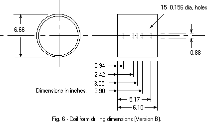
The coil should be mounted with its axis
at a 30 degree angle to the front panel as shown in Fig.1. The center
of the coil form is 2 7/8" back from the rear edge of the baseboard and
5 5/8" to the left of its right edge. These dimensions are
important, as is the actual size of the breadboard, if one wishes to
construct a double-tuned four band crystal radio set out of two Version
'b' single-tuned four band crystal radio sets as described in Article
#23.
The diode: This design is optimized for use with a diode having an n of 1.03 and a Saturation Current (Is) of about 82 nA, although this is not critical and other diodes can be used with good results. See Articles #0, #4 and #16 for info on n and saturation current (Is) of diodes, and how to measure them. If desired, and one has a favorite diode, its effective (Is) can be changed by applying a DC bias voltage, using perhaps, the 'Diode Bias Box' described in Article #9. One suitable diode, the published parameters of which show an (Is) of 100 nA is a Schottky diode, the Agilent HBAT-5400. It is a surface-mount unit that was originally designed for transient suppression purposes. Measurements of many HBAT-5400 diodes seems to show that there are two varieties. One type measures approximately: n=1.03 and (Is)=80 nA. The other type seems to have an n of about 1.16 and an (Is) of about 150 nA. Both work well but the former works the best. This part, available in an SOT-23 package is easily connected into a circuit when soldered onto a "Surfboard" such as manufactured by Capital Advanced Technologies (http://www.capitaladvanced.com/), distributed by Alltronics, Digi-Key and others. Surfboard #6103 is suitable. The HBAT-5400 is also available in the tiny SO-323 package that can be soldered to a 330003 Surfboard. The Agilent HSMS-2860 microwave diode (Specified Is=50 nA) is available as a single or triple with three independent diodes in the SO-323 and SO-363 packages, respectively. The Agilent number for the triple diode is HSMS-286L. I find it to be particularly good for DX in this crystal radio set. It is a convenient part since one can connect it using only one section (shorting the unused ones) or with two or three in parallel. This gives one a choice of nominal saturation currents of 50, 100 or 150 nA. Samples of this part I have tested measured about 35 nA per diode, not 50. I don't know the normal production variations. The only disadvantage of this diode, as far as I know, is its low reverse breakdown voltage which may cause distortion and low volume on very loud stations. It has the advantage, as do most Schottkys, of having much less excess reverse leakage current than do germanium diodes. This helps with volume and selectivity on very weak stations. Infineon makes a BAT62 Schottky diode in several different quite small surface mount packages. The single BAT62 is physically the largest. It has a specified (Is) of about 100 nA and performs quite well. Be forewarned that the diode parasitic series resistance is a high 100 ohms in this diode. A resistance even this high should not have a noticeable effect on the performance of a crystal radio set. Most germanium diodes have too high a saturation current for the best selectivity and should to be back-biased or cooled for optimum performance. See Article #17A for more info on this. Different type diodes may be connected to the terminals labeled Diode #1 and Diode #2, with either one selectable with SW6. When one diode is selected, the other is shorted. This feature makes it easy to compare the performance of a 'test' diode with one's 'favorite' diode. Another use is to place one's best DX diode in one position and one having a very low reverse leakage resistance at high reverse voltages in the other. This will maximize strong signal volume and minimize audio distortion. A good choice for this crystal radio set is a diode having a relatively low saturation current such as 3 or 4 Agilent HSMS-2820 or HSMS-2860 diodes in parallel as Diode #1 for high selectivity and sensitivity on weak signals, and an Agilent HBAT-5400 or one of the lower saturation current germaniums as Diode #2 for low distortion and maximum volume on strong stations. Don't use two diodes in series if you want the best weak signal sensitivity in any crystal radio set. The result of using two identical diodes in series is the simulation of an equivalent single diode having the same (Is) but an n of twice that of either one. This reduces weak signal sensitivity. The inductor for this single tuned crystal radio set is made up of the four closely coupled inductors L1, L2, L3 and L4. The inductance from point A to ground (Fig. 5) is 250 uH when SW3 is in the 'up' position (used for low band reception) and 62.5 uH in the 'down' position (used for high band reception). Better performance from a higher tank Q at the high frequency end of band B may be obtained by using the "contra-wound" coil winding technique described in Article #26. This minimizes distributed coil capacitance in band B as opposed to the winding connections used here that minimize coil distributed capacity in band A. Audio impedance transformation from the audio output resistance of the diode detector to 'series connected' 1.2k ohm sound-powered phones is provided by the audio transformers. If one wishes to use 300 ohm sound-powered phones with two 600 ohm elements connected in parallel instead of series, a very good low loss transformer choice is the 100k-100 ohm transformer from Fair Radio Sales, #T3/AM20. The configuration of two Calrad transformers shown on line 2 of the Calrad chart in Article #5 is also a good choice. C11, along with the shunt inductance of the transformer and the inductance of the sound powered phones form a high-pass filter, hopefully flat down to to 300 Hz. R3 is used to adjust the DC resistance of the diode load to the AC impedance of the transformed effective AC headphone impedance. C10 is an audio bypass. The two variable capacitors C7 and C8 interact substantially when tuning a station. C7 mainly controls the selectivity and C8 mainly controls the resonant frequency. If the antenna-ground system being used has a resistance larger than 25 ohms, C7 will have to be set to a smaller capacitance in order to maintain the proper resonant resistance at point A in Fig. 5. If the capacitance of the antenna-ground system is greater than 200 pF, C7 will also have to be set to a lower value than if it were 200 pF. The "capacitive" attenuators controlled by SW1 and SW2, used for volume and selectivity control, are designed so as to cause minimal tank circuit detuning when the equivalent circuit of the antenna-ground system used has the same values as the old IRE simplified Dummy Antenna recommended for testing Broadcast Band radio receivers. It consisted of a series combination of a 200 pF cap, 20 uH inductor and a 25 ohm resistance. The geometric mean of the sum of the reactances of the capacitor and inductor at 520 and 1710 kHz is (-605) ohms. This is the reactance of a 279 pF capacitor (characteristic capacitance of the "capacitive" attenuator) at 943 kHz, the geometric mean of the BC band of 520-1710 kHz. The "capacitive" attenuators were designed for the specified attenuation values (15 and 30 dB) utilizing the 500 ohm resistive pi attenuator component values table shown in the book "Reference Data for Radio Engineers". The resistor values for 15 and 30 dB "capacitive" attenuators were normalized to 605 ohms, then the "capacitive" attenuator capacitor values were calculated to have a reactance, at 943 kHz, equal to the value of the corresponding "capacitive" attenuator shunt or series resistance. Since the "capacitive" attenuators, when switched into the circuit, isolate the antenna-ground system resistance from the tank circuit, selectivity is increased. This is a convenient feature, since less retuning is required than if selectivity is increased by reducing C7 and increasing C8. If the series capacitance of the equivalent circuit of one's own antenna-ground system is 200 pF, at 943 kHz, practically no retuning is required. If the equivalent L and C of one's own antenna-ground system differ substantially from those of the simplified IRE dummy antenna used here, one can normalize the values of the capacitors used in the "capacitive" attenuators to match ones's own antenna-ground system. A method for measuring the parameters of one's own antenna-ground system is shown in Article #20. 4. 'Loop Effect' of the tank
inductor, and how it can be used to tame One can use local signal pickup by the tank (loop effect) to reduce the effect of interference from strong stations by rotating the crystal radio set about a vertical axis. The correct angle will generally reduce it. 5. How to improve selectivity with a relatively small loss in sensitivity.
Note: When altering selectivity by changing switch
positions, always re-balance the relative settings of C7 and C8. 6. Just how loud is a station that delivers the amount of power necesssary to operate the Diode Detector at its 'Crossover Point' between Linear and Square-Law Operation? Many Articles in this series have talked about the 'Linear-to-Square-Law Crossover Point' (LSLCP). Please bear in mind that the LSLCP point is a point on a graph of output DC power vs input RF power of a diode detector system. It is not a point on a graph of DC current vs voltage of a diode. Two things can be said about a detector when it is fed a signal that operates it at its LSLCP. (1) A moderate increase of signal power will move the detector into its region of substantially linear operation. (2) A similar moderate decrease of input power will move it closer to its region of substantially square law operation, where a 1 dB decrease of input power results with a 2 dB decrease of output power. For more info on the LSLCP, see Article #15A. The crystal radio set described in this Article is operating at its LSLCP if the rectified DC voltage at the 'Diode Bias' terminals is 53 mV, a diode having a Saturation Current (Is) of 82 nA and an ideality factor (n) of 1.03 is used (such as a selected Agilent HBAT-5400), and if R3 is set to 325k ohms. At this point the diode rectified current equals two times its Saturation Current. The volume obtained is usually a low to medium, easy-to-listen-to level. 7. 'Short Wave ghost Signal', 'background hash' and spurious FM reception. All single tuned crystal radio sets may be, in fact, considered double tuned (except single tuned loop receivers). The second response peak arises from resonance between the equivalent inductance of the antenna-ground system and the impedance it sees, in this case, the series combination of capacitors C7 and C8. This peak usually appears at a frequency above the broadcast band and gives rise to the possibility of strong so-called 'short wave ghost' signal interference when a short wave station has a frequency near the peak . The response at this ghost frequency can be made somewhat weaker and moved to a higher frequency if the antenna-ground system inductance is reduced. One can use multiple spaced conductors for the ground lead to reduce its inductance. I use a length of TV 300 ohm twin lead, the two wires connected in parallel for this purpose. Large gauge antenna wire, or spaced, paralleled multiple strands helps to reduce the antenna inductance (flat top antenna). If the down-lead is long compared to the ground lead, use multiple, paralleled, spaced conductors to reduce its inductance (similar to using a 'cage' conductor). Another possible cause of 'ghost' signal reception resides in the fact that the response of the so-called single tuned circuit does not continuously drop above resonance as frequency rises, but only drops to a relatively flat valley before rising again to the second peak. The frequency response above the main (lower) peak would drop monotonically (true single tuned operation) if the second peak did not exist. The relatively flat response valley that exists between the two peaks, provides the possibility (probably likelihood) of interference 'hash' if several strong stations are on the air at frequencies in the valley range. It also is the cause of a strong local station, above the frequency of a desired station "riding through" and appearing relatively constant even if the tuning dial is moved. The response should drop at a 12 dB per octave rate above the second peak. A useful side effect of the response behavior of this type of circuit is that the response below the main resonance drops off at an extra fast rate of 12 dB per octave rate instead of an expected 6 dB. The most effective way to substantially eliminate 'short wave ghost' and hash reception is to go to a double-tuned circuit configuration or to use traps. Spurious FM reception caused by so-called FM 'slope' detection can occur from close by local FM stations if a spurious FM resonance appears somewhere in the circuitry of a crystal radio set. If ground wiring is not done properly in the crystal radio set, spurious signals can get into the detector. The thing to do here is to run all the RF and audio grounds to one point as shown in Fig.5. Sometimes a small disc bypass capacitor, 22 pF or so, placed across the diode will help. Another way to try to reduce FM interference is to put a wound ferrite bead 'choke' in series with the antenna and/or ground leads. In order not to affect normal BC band reception, the resultant ferrite inductor should have a reasonable Q and a low inductance in the BC band. It should also exhibit a high series resistance at FM frequencies. Suitable wound ferrite chokes (bead on a lead) are made by the Fair-Rite Corp. as well as others. Two types available from Mouser are #623-29441666671 and #623-2961666671. This suggestion may also help reduce "short wave ghost" signal reception. 8. Some simulated and actual measurements on the crystal radio set.
Fig. 7 shows the simulated frequency response at the center of the LoLo band, from the antenna source to the RF input of the diode. The red graph and figures in the left panel show an insertion power loss of 2.4 dB with a -3 dB bandwidth of 6 kHz, along with the spurious response peak at 4.4 MHz, caused by the antenna-ground system inductance. The insertion loss at the spurious peak is 15 dB. The loss in the valley is 40 dB. The right graph and figures show the Input Return Loss (impedance match) at resonance to be -12.2 dB. The output return loss (not shown) is the same. Fig. 8 shows the simulated frequency response at the
center of the HiHi band, from the antenna source to the RF input of the
diode. The red graph and figures in the left panel show an insertion
power loss of 4.1 dB with a -3 dB bandwidth of 6 kHz, along with the
spurious response peak at 6.9 MHz, caused by the antenna-ground system
inductance. The insertion loss at the spurious peak is 20 dB. The loss
in the valley is 47 dB. The right graph and figures show the Input
Return Loss (impedance match) at resonance to be -8.5 dB. The output
return loss is the same.
9. A method for measuring the unloaded Q of an L/C resonator.
10. Important information re: unloaded tank Q. Every effort should be made to achieve as high an unloaded tank Q as possible, in order to minimize RF loss at the desired -3 dB bandwidth (selectivity), and especially when using narrower bandwidths. Somewhat greater insertion power loss and/or broader selectivity may result if components having a greater dielectric loss than those specified are used. Sensitive areas for loss are:
11. Measurements.
In use, C7 and C8 are usually set to different values to achieve the design-bandwidth of 6-7 kHz. However, if they are set to the same values, a frequency calibration chart can be made for each band as shown above. The bold figures indicate the approximate position of each band when the crystal radio set is driven by the standard antenna-ground system. There is sufficient extra capacitance range available in C7 and C8 to handle antenna-ground systems that differ substantially in impedance from the standard dummy antenna used in the design.
The data in Table 4 shows the insertion power loss in the crystal radio set when driven by an RF signal that is amplitude modulated at 50% by a 400 Hz sine wave. See Article #11 on how to measure the insertion power loss and bandwidth of a crystal radio set. The audio output power was set to -70 dBW for each reading. The available carrier input power supplied to the crystal radio set was about -60 dBW, with a total available sideband power of about -66 dBW. The audio output power is that delivered by the diode detector to the audio load and does not include losses in an audio transformer. One should add about 1.0-1.5 dB to the insertion power loss shown in Table #4 to allow for audio transformer loss. The reason the audio transformer loss does not show up in the measurements is that the audio transformers (T1 and T2) were not used. SW7 was placed in the UP position, providing a direct high impedance output from the diode detector. The Zero Loss Unilateral 'Ideal Transformer' Simulator described in Article #14 was used to provide a 320k to 1200 ohm impedance transformation, close to that provided by T1 and T2 in actual crystal radio set operation. Note: The diode rectified DC voltage at the power levels used above is 0.51 volts. At this power level, a SPICE simulation of the detector shows a theoretical diode detector insertion power loss of 1.4 dB. |
|||||||||||||||||||||||||||||||||||||||||||||||||||||||||||||||||||||||||||||||||||||||||||||||||||||||||||||||||||||||||||
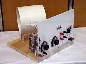
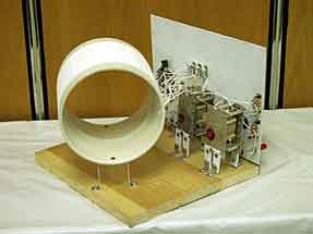
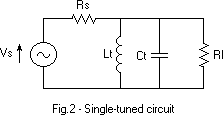
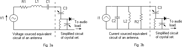
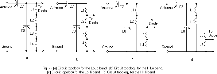
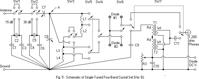


Selectivity and sensitivity are essentially constant
over the entire AM broadcast band because of the use of 'Benodyne'
constant bandwidth antenna coupling, resonant impedance control and band
splitting. The coupling coefficient of the resultant double tuned
circuit is easily adjustable from greater than critical coupling to
approximately zero. Insertion power loss varies from about 4.5 to 6.5
dB at the center of each of the four bands (including the diode detector
loss but excluding audio transformer loss). Selectivity is quite
sharp: -3 dB bandwidth is 6-7 kHz and -20 dB bandwidth varies from 16
to 22 kHz. The average ratio of the -20 dB to the -3 dB bandwidth is
3.0. This is the same as the theoretical value shown on a graph in
Terman's Radio Engineer's handbook, page 160, for two critically coupled
circuits resonant at the same frequency and having a Q ratio of unity.
Operation can be quickly changed to that of a single tuned crystal radio
set accompanied by a sharp and deep tunable trap. The tank inductor in a VbST4BCS is mounted so that its axis makes a 30 degree angle with the front panel. This orientation enables the magnetic coupling between two VbST4BCS tuned circuits to be easily varied from above critical coupling down to about zero. Incidentally, if one uses two identical coils, wound in the same direction and positioned as recommended in Article #22, the capacity coupling between the coils will be phased such as to partially oppose the magnetic coupling. To create a DT4BCS, two VbST4BCS are placed side-by-side next to each other with baseboards touching each other. The coupling between the two tuned circuits can be varied by sliding one VbST4BCS forward or back compared with the other. If one is starting from scratch and is only interested in having a double-tuned crystal radio set, unnecessary parts may be removed from each of the VbSt4BCS units as follows:
If one is interested in having a single-tuned crystal
radio set as well as a double tuned one, one full VbST4BCS may be used
with either of the reduced parts count units #1 or #2 above.
2. Operation of a DT4BCS when two VbST4BCS units are used. Connect antenna and ground to unit #1. Position SW1 and SW2 at their 0 dB settings. Make sure no diode is connected to either the Diode #1 or Diode #2 terminals of unit #1. Connect phones to unit #2. Connect a detector diode to either of the two diode terminal pairs of unit #2 and switch it into the circuit using SW6. In set #2, set SW1, SW2 to activate their attenuation, and C7 to minimum capacitance. Select one of the four bands for listening and set SW3, SW4 and SW5 in set #2 appropriately, as described in Table 1 in Article #22. Set SW3 in unit #1 to its up position when using bands LoLo and HiLo and its down position when and for using bands LoHi and HiHi. Listening is usually done using critical coupling between the two tuned circuits. This occurs in the Lo band when the front panel of unit #2 is placed about 2 7/8" back from that of unit #1. The figure for the Hi band is about 3 3/4 ". Almost complete cancellation of coupling occurs when the front panel of unit #2 is pushed about 5 3/8" back from that of unit #1. Tune in a station using C7 and C8 of unit #1 and C8 of unit #2. Greater selectivity is possible if needed. See Part 5 of Article #22 for more info on this. If interference is a problem, try reducing coupling below critical by moving set #2 further back. Very important: Optimum operation and best selectivity occurs when the loaded tank Q of unit #1 equals that of unit #2. A way to check for for this is to tune in a station and lightly place a finger on the stator (point A in Fig. 5 of Article #22) of C8 of unit #1, then on C8 of unit #2. If similar decreases of volume occur, the Qs are about equal. If the volume is reduced more by touching C8 of unit #1 than unit #2, increase C7 of unit #1 somewhat, restore tuning with C8 and try again. If the volume is reduced more touching C8 of unit #2 than unit #1, decrease C7 somewhat, restore tuning with C8 and try again for equal effects. If a strong local station seems to 'bleed through' the
tuned circuits, that may be because the inductor of unit #2 is acting as
a loop antenna and picking it up. One way to reduce this problem is to
rotate the unit #1-unit #2 assembly about a vertical axis and attempt to
null out the pickup. Another approach could be to make physically
smaller coils while still maintaining (or increasing) Q by using litz
wire or by adding a trap.
Note: The diode rectified DC voltage at the power levels used in the measurements above is 0.5 volts (Rheostat R3 set to 350k ohms). At this power level, a SPICE simulation of the detector shows a theoretical diode detector insertion power loss of about 1.4 dB. |
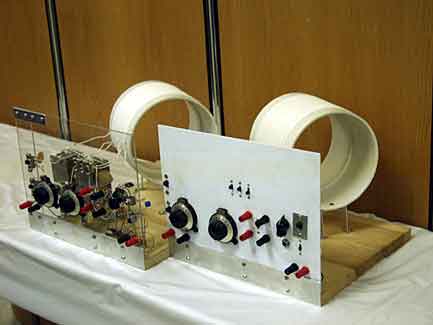
|
||||||||||||||||||||||||||||||||||||||||||||||||||||||||||||||||||||||||||||||||||||||||||||||||||||||||||||||||||||||||||||||||||||||||||||||||||||||||||||||||||||||||||||||||||||||||||||||||||||||||||||||||||||||||||||||||||||||||||||||||||||||||||||||
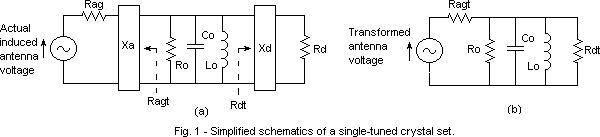
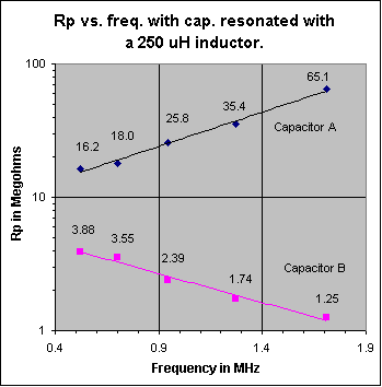
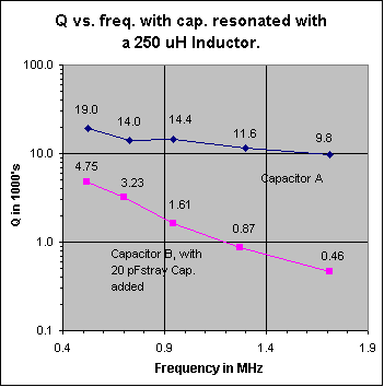
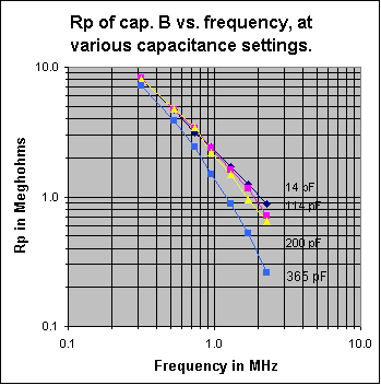
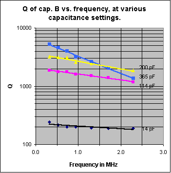
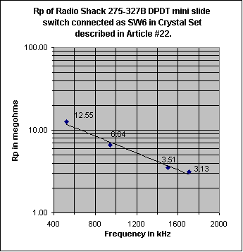
|
A new approach to amplifying the output of a crystal radio set, using energy extracted from the RF carrier to power a micro-power IC to drive headphones or a speaker The Amplifier, applied to a crystal radio set: This crystal radio set operates in the same manner as the ones described in Articles #22 (Benodyne version B)and #26 (Benodyne version C) when switches SW7 and SW 8 are in their 'up' positions and SW9 is to the right. To operate the amplifier, first, supercapacitor C13 must be charged up to at least 1.5 volts. The manufacturer of the IC specifies a minimum of 1.8 volts, but so far, I have found that 1.5 volts to be sufficient. To charge C13, set SW7 and SW8 to their 'up' positions, SW9 to the right, and the wiper arm of R3 to the center (see Fig. 1). Tune in a station that provides between 1.3 and 5 .5 volts DC at the 'Detector bias monitor' terminals. If the voltage is too low, try changing the antenna impedance matching by optimizing the settings of C7 and C8. Set SW7 to its down position and C13 will start charging. If no station exists that is strong enough to supply at least 1.5 volts, C13 may be charged by connecting a series combination of a 4.5 volt battery and a 100 ohm current limiting resistor across it for about 30 minutes. Make sure the + side of C13 is charged positive. After C13 is charged, set SW7 to its up position. The higher the final charged voltage on C13, the higher the maximum volume will be. Non-amplified operation with Sound Powered 1200 ohm headphones: SW7 and SW8 are up and SW9 is to the right. R3 is used to optimize DC current in the diode for minimum audio distortion. Amplified operation with Sound Powered 1200 ohm headphones on very weak signals: SW7 is up, SW8 down and SW9 is to the right. Amplified operation, driving an 8 of 16 ohm speaker from medium and strong stations: Operate SW7 to its up position, SW8 down and SW9 to the left. The speaker will probably give forth with some distorted audio. To reduce the distortion, try adjusting R3. If this doesn't help enough, reduce the signal into the amplifier. The attenuators, controlled by SW1 and/or SW2 can be used to do this (see Fig. 1). If no SW1 or SW2 is present, reduce the output of the detector by decoupling the antenna (reduce C7 and restore tuning using C8). Switch SW10 provides a tradeoff between maximum volume and current drain. Switching to the white wire connection gives the, longest listening time, but with a lower maximum volume. Each listener must make his own choice here. The current drain from C13 and the life of its charge are directly proportional to the strength of the audio signal and the setting of SW10. Maximum low-distortion volume is proportional to the voltage charge on C13. For comparison purposes with receiving locations other than mine, there are two 50 kW stations about 10.5 miles from my home. They are WOR and WABC. My attic antenna is described in Article #20. Either station can deliver about a 5.0 volt charge to C13. This crystal radio set was constructed by modifying a Version 'b' crystal radio set (See Article #22), using the air-mounted, flying joint method of wiring the amplifier components. A convenient way to connect to the tiny leads of IC1 is to first solder it to a surfboard such as one manufactured by Capital Advanced Technologies (http://www.capitaladvanced.com). Their models 9081 or 9082 are suitable and are available from various distributors such as Alltronics, Digi-Key, etc. The amplifier can be built in as an addition to any crystal radio set if proper allowance is made for impedance matching considerations. Charge/discharge considerations for C13: C13 (0.33 F) will charge close to full capacity after about 24 hours of charging. The first charge will not last as long as subsequent ones because of a phenomenon known as "dielectric absorption". If C13 is reduced to 0.1 F, about 8 hours are needed. Listening time when using headphones should be greater than 24 hours when using 0.33 F, and 10 hours when using a 0.1 F value. There is a greater current drain on C13 when using a speaker, and the listening time will depend upon the volume setting. Listening times approximate 10 hours when using a 0.33 F cap and 3 hours when using 0.1 F.
Parts List when the crystal radio set used is the
that described in Article #22. The amplifier is
** For lower cost, the following component substitutions may be made: Together they cause a small reduction in performance at the high end of the band (1.75 dB greater insertion power loss and 1.5 kHz greater -3 dB bandwidth). The performance reduction is less at lower frequencies.
|
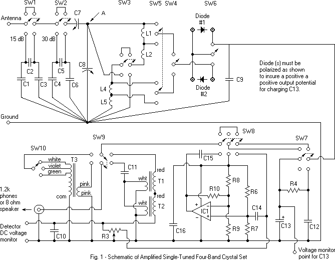
|
Highly sensitive and selective single-tuned
four-band crystal set using a new contra-wound dual-value inductor,
and having a "sharp selectivity setting"; along with a way to
measure the unloaded Q of an L/C resonator
Selectivity and insertion power loss figures from a computer simulation are given and compared with those of the actual physical crystal radio set. A way to tell if the detector is operating below, at or above its 'Linear-to-Square Law Crossover point' (LSLCP) is described. See Article #15a for a discussion of LSLCP. No antenna tuner is necessary for the average outdoor or attic antenna. An explanation of 'short wave ghost signals' and 'hash' is provided along with some suggestions on how to combat them. Version C uses a tank coil constructed with litz wire, as compared to the solid teflon insulated wire used on version 'B'. A new way to make a higher Q, low inductance coil is described. Some additional benefits of the "Benodyne" type of tank
circuit are: (1) Reduction of the the sharp drop in tank Q or
sensitivity at the high frequency end of the BC band often experienced
when only one value of tank inductance is used for the whole BC band.
(2) Reduction of the tank Q loss from the variable cap when using lower
cost units that use phenolic insulation, such as the common 365 pF cap
(see Figs. 2, 3, and 4 in Article #24). The "two inductance value
benodyne* circuit is used in the crystal radio sets in Articles #22 and
#26. We will assume here that the two "benodyne" component inductors
(see "The Tank Inductor" in this Article) provide a tank inductance of
250 uH in the low frequency half of the BC band (520-943 kHz) and 62.5
uH in the high half (0.943-1.71 MHz). If the large 250 uH inductance
setting were used all the way up to the top end of the BC band (as in
the usual case), a total tuning capacity of 34.7 pF would be required at
1.71 MHz (Condition A). In the "Benodyne" circuit, with the 62.5 uH
inductance setting used for the high frequency half of the BC band, a
total tuning capacitance of 139 pF is required at 1.71 MHz (Condition
B). Benefit (1) occurs because in condition A, a larger fraction of the
total tuning capacitance comes from the typically low Q distributed
capacity of the inductor than in condition B. This results in a higher
Q total capacitance in condition B than in condition A. Benefit (2)
occurs because the effective Q of a typical 365 pF variable cap, when
used with a 250 uH tank, is about 500 at 1.71 MHz (see Fig. 3 in Article
#24). The Q of the 365 pF variable cap, when set to 139 pF, is greater
than 1500 (see Fig.5 in Article #24). This higher Q results in less
loss and greater selectivity at the high end of the BC band in condition
2. A further benefit of the Benodyne circuit at the high end of the BC
band is greater immunity from the Q reducing effects of surrounding high
loss dielectric materials such as baseboard etc. The lossy stray
capacity introduced is better swamped out by the high shunt tuning
capacity used. The Crystal Radio Set Design, in a (large) Nutshell:
Fig. 1 - Single-Tuned Four-Band
Crystal Radio Set, Version 'C'. These are actually pictures of Version
B as Design objectives:
1. Theory 
The frequency response shape of the circuit shown in Fig. 2 is that of a simple single tuned circuit and can be thought of as representative of the nominal response of a single tuned crystal radio set. Consider these facts:
2. Design Approach for the Center of each of the four sub-bands. 
Fig. 3a shows the simplified Standard Dummy Antenna circuit, described in Terman's Radio Engineer's Handbook for simulating a typical open-wire outdoor antenna-ground system in the AM band. R1=25 ohms, C1=200 pF and L1=20 uH. See Article #20 for info on how to measure the resistance and capacitance of an antenna-ground system. These values are used in the design of the crystal radio set. R1 represents the antenna-ground system resistance, C1 the capacitance of the horizontal wire and lead-in to ground and L1 represents the series inductance of the antenna-ground system. The values of R1, C1 and L1 in Fig. 3a are considered to be independent of frequency. To the extent that they may vary with frequency, C7 and C8 in Fig. 4 can be adjusted to compensate. The current-source equivalent circuit of the antenna-ground circuit is shown in Fig. 3b. To a first degree of approximation, C2 in Fig. 3b is independent of frequency. R2 will vary approximately inversely with frequency. We will ignore the effect of L2, since its value is large, except when approaching the first resonance of the antenna-ground system. The design approach is to place a variable capacitor C3 in series with the antenna circuit (Fig. 3a) to enable impedance transformation of the antenna-ground circuit to an equivalent parallel RC (Fig. 3b), the R component of which can be adjusted by changing the value of the C3 to follow a desired relationship vs frequency. One of the objectives of the design is to enable as constant a bandwidth as possible vs. frequency. This requires the aforementioned equivalent parallel component (R2) to vary proportionally with the square of the frequency if capacitive tuning is used in each sub-band (loaded Q must be proportional to frequency for a constant bandwidth). The shunt variable capacitor to ground, shown across the tank coil, is used to tune the tank to resonance. This design attempts to accomplish this in the center of each sub-band. Performance is close at the band edges. 3. The single tuned crystal radio set The topology of the single tuned circuit is changed from band to band as shown in Fig. 4 below.
Resonant RF resistance values at the top of C8 (Fig. 4) from antenna loading are designed to be: 250k ohms at the center of sub-bands 1 and 3 and 500k ohms for sub-bands 2 and 4. Since the diode is tapped at the 0.7 voltage point for bands 2 and 4, it sees a source resistance at resonance of: 125k for sub-bands 1 and 3 and of 250k ohms for sub-bands 2 and 4. These figures apply for the theoretical case of zero loss in the tuned circuit components (infinite Q). In a shunt capacitively tuned crystal radio set, loaded with a constant resistive load, the bandwidth will vary as the square of the frequency. To understand why, consider this: When the resonant frequency of a tuned circuit loaded by fixed parallel resistance is increased (from reducing the total circuit tuning capacitance), the shunt reactance rises proportionally, giving rise to a proportionally lower circuit Q. But, a proportionally higher Q is needed if the bandwidth is to be kept constant. Therefore, the square relation. In the practical case, we are faced with two problems. (1) How should we deal with the fact we work with finite Q components? (2) At high signal levels (above the LSLCP), the RF load presented by the diode to the tuned circuit is about 1/2 the audio load resistance, and at low signal levels (below the LSLCP) the RF load presented by the diode is about 0.026*n/Is ohms. Compromises are called for.
Parts List - All components are chosen for the best possible sensitivity at a -3 dB RF bandwidth of 5-6 kHz.
** For lower cost, the following component substitutions may be made: They cause a reduction in performance at the high end of the BC band, especially, sub-band 4 when the "narrow selectivity" setting is used. Performance reduction is much less in the lower sub-bands and in the "normal selectivity setting.
Wiring the crystal radio set: The stator and rotor terminals of C8 are labeled points A and B (see Fig. 5), and all connections to them should be short and direct. The purpose is to minimize spurious FM and short-wave resonances which might be created otherwise. This approach eliminates as much wiring inductance associated with C8 as possible, maximizing its ability to shunt out any high frequency spurious responses that might be present. Some more info on this subject is presented near the end of part 8. The 'contra-wound' tank inductor: L1, L2, L3 L4 and L5 are all components of the tank. It is wound with litz wire having 660 strands of #46 conductor. L1 has 13 turns, L2 has 3.125 and L3 has 8.875, all close wound (because the form is not long enough to enable spacing and the extra turns that would be required to maintain the inductance) as component inductor #L(1,2,3) with two taps. L4 has 7.25 turns and L5 has 17.75, both close wound as component inductor #L(4,5) with one tap. The start of L1 of component inductor #L(1,2,3) is spaced 0.06" to the right of the center of the coil form, looking at the crystal radio set from the front and winding continues through L2 and L3 clockwise to about 0.25" of the right end of the form, looking at the crystal radio set from the right. The start of L4 of component inductor #L(4,5) is spaced 0.06" to the left of the center of the form, looking at the crystal radio set from the front and winding continues through L5 clockwise to about 0.25" of the left end of the form, looking at the crystal radio set from the right. When one looks at a completed contra-wound inductor, one can see that the component inductors #L(1,2,3) and #L(4,5) are wound in opposite directions. Note: All coil dimensions are measured from turn center to turn center. See Article #0, Part 12 for a mini-Article about the purpose and use of the 'contra-wound' inductor. Figures 2 and 3 in Article #29 provide more info on the contra-wound inductor approach. Here is the reason for this winding scheme: One can see from Fig. 4 that this crystal radio set design connects component inductors #L(1,2,3) and #L(4,5) in series for the lower half of the BC band and in parallel for the upper half. If the two coils were wound in the same direction from the hot to the cold end, as was done in the crystal radio set described in Article #22, distributed capacitance would be low in the series connection (about 7.7 pF) and higher in the parallel connection (about 21 pF), mainly because the finish (ground end) of component inductor #L(1,2,3) is located close to the start (hot end) of component inductor #L(4,5). This reduces the Q at the high end of the BC band. If the coils are contra-wound, as I call it, the lower distributed capacitance condition occurs in the parallel, not the series connection, resulting a Q increase of approximately 17% at 943 kHz. It is increased even more at the high end of the BC band. The coil form is made of high-impact styrene. OD=4.5", ID=4.22" and length=3.625". I used part #S40140 purchased from the Genova Products factory retail store. (http://genovaproducts.com/factory.htm). A PVC form can be used, but its dielectric has about 4-5 times the loss of the styrene form and will reduce Q, especially at the high end of the BC band. The start (hot) ends of L1 and L4 are affixed to the form by being lead through two 0.25" diameter holes placed 0.5" apart, measured in the circumferential direction, and held in place by 0.5" wide film tape on the inside of the form. The finish (cold) ends of L3 and L5 are affixed to the form by being lead through two 0.125" holes placed 0.5" apart, measured in the circumferential direction, and held in place as above. Three 0.125" diameter holes spaced 0.5" apart are used when pulling a tap. In Fig. 6, the red line represents the litz wire and the yellow arcs represent a cross-section of the coil form through the center of the 0.125 or 0.25" holes.
Fig.7 Coil mounting hardware. To wind the tank coil, first cut five pieces of 660/46 litz as follows: For L1: 16' 9", L2: 4' 3", L3: 11' 10", L4: 9' 11" and L5: 22' 5". These lengths provide about 9" of free length at each end. The ends of each wire length should be tinned to prevent unraveling of the strands and serving while winding the coils. Use a small Weller WC-100 adjustable temperature iron (or equivalent), set to maximum temperature (really hot!) for tinning. The method is to immobilize an end of the wire end by extending it about 2" over the end of a table and placing a weight on top of it. One can then apply the very hot iron tip to the cut strand ends and feed in a little solder to wet them. As the heat percolates down the litz and the insulation burns off or melts, more solder can be applied a little further down and around the end to obtain a solid tinning for a lead length of about 0.25". If one don't want an inch or so of litz beyond the solder to become stiffened from melted insulation, one might do as John Davidson has suggested. He tightly wraps a length of aluminum foil around the litz, up to 0.375" from the end before soldering to act as a heat sink and keep the insulation cool. I haven't tried this out. The start leads of L1 and L4 should be spaced 0.06", right and left from the longitudinal center of the coil form. One can use a bent up plastic soda straw in the 0.25" holes to keep the wires approximately in place). Gradually taper the wires further apart going through the first turn, then to become close wound for the remainder of the windings. Table 1 - Longitudinal locations for the taps and start/finish of L1, L2. L3, L4 and L5.
After the windings are completed, one should have a coil with ten droopy wires coming from it. The next step is to tidy up the coils, adjust the 0.12" wire spacing at the start of L1 and L4 and their one-turn taper. Move any excess winding space to slightly space-wind the last several turns of L3 and L5 at their finishes (cold ends). The turns should then be sprayed with one light application of crystal clear "Krylon" acrylic lacquer, Rust-Oleum Specialty high luster lacquer coating (clear) or equivalent, to hold them in place. The ends of L1 through L5 that are to be joined to form the taps should be cut to a length of about 0.5", tinned and soldered together as shown in Fig. 6. Pigtails for wiring to the switches should now be soldered to the taps. The coil form should be mounted with its axis parallel to the front panel as shown in Fig.1, its center about 6.50" back, and centered horizontally. Tank coil specs. for those who wish to use a different diameter coil form, axial length of total winding, wire size or wire to wire spacing:
The diode: This design is optimized for use with a diode having an n of 1.03 and a Saturation Current (Is) of about 106 nA at 25° C., although this is not critical and other diodes can be used with very good results. See Articles #0, 4 and 16 for info on n and Is of diodes, and how to measure them. If one has a favorite diode, its effective (Is) can be changed by applying a DC bias voltage, using perhaps, the 'Diode Bias Box' described in Article #9. An excellent diode to use in this set is the ITT FO-215 germanium unit that was made 20 or so years ago (see Article #27). NOS may be available from from Dave Schmarder at http://www.1n34a.com/catalog/index.htm and Mike Pebble at http://www.peeblesoriginals.com Another suitable diode, the published parameters for which show an (Is) of 100 nA is a Schottky diode, the Agilent HBAT-5400. It is a surface-mount unit that was originally designed for transient suppression purposes. Measurements of many HBAT5400 diodes seem to show that there are two varieties. One type measures approximately: n=1.03 and (Is)=80 nA The other type seems to have an n of about 1.16 and an (Is) of about 150 nA Both work well but the former works best. This part, available in an SOT-23 package is easily connected into a circuit when soldered onto a "Surfboard" such as manufactured by Capital Advanced Technologies (http://www.capitaladvanced.com/), distributed by Alltronics, Digi-Key and others. Surfboard #6103 is suitable. The HBAT5400 is also available in the tiny SO-323 package that can be soldered to a 330003 Surfboard. The Agilent HSMS-2860 microwave diode (Specified Is=50 nA) is available as a single or triple with three independent diodes in the SO-323 and SO-363 packages, respectively. The Agilent number for the triple diode is HSMS-286L. I find it to be particularly good for DX in this crystal radio set. It is a convenient part since one can connect it using only one section (shorting the unused ones) or with two or all three in parallel. This gives one a choice of nominal saturation currents of 50, 100 or 150 nA Samples of this part I have tested measured about 35 nA per diode, not 50. I don't know the normal production variations. The only disadvantage of this diode, as far as I know, is its low reverse breakdown voltage which may cause distortion and low volume on very loud stations. It has the advantage, as do most Schottkys, of having much less excess reverse leakage current than do germanium diodes. This helps with volume and selectivity on very weak stations. Infineon makes a BAT62 Schottky diode in several different small surface mount packages. The single BAT62 is physically the largest and easiest to handle. It has a specified (Is) of about 100 nA and performs quite well. Most germanium diodes have too high a saturation current for the best selectivity when receiving weak signals and should to be back-biased or cooled for optimum performance, although the difference is usually hard to notice. See Article #17A for more info on this. Different type diodes may be connected to the terminals labeled Diode #1 and Diode #2, with either one selectable with SW5. When one diode is selected, the other is shorted. This feature makes it easy to compare the performance of a 'test' diode with one's 'favorite' diode. Another use is to place one's best DX diode in one position and one having a very low reverse leakage current at high reverse voltages in the other. This will maximize volume and minimize audio distortion on strong signals. A good choice for this crystal radio set is a diode having a relatively low saturation current such as 3 or 4 Agilent HSMS-2820 or HSMS-2860 diodes in parallel as Diode #1 for high selectivity and sensitivity on weak signals, and an Agilent HBAT5400 or one of the lower saturation current germaniums as Diode #2 for low distortion and maximum volume on very strong stations. Don't use two diodes in series if you want the best weak signal sensitivity in any crystal radio set. The result of using two identical diodes in series is the simulation of an equivalent single diode having the same (Is) but an n of twice that of either one. This reduces weak signal sensitivity. Different type diodes may be connected to the terminals labeled Diode #1 and Diode #2, with either one selectable with SW5. When one diode is selected, the other is shorted. This feature makes it easy to compare the performance of a 'test' diode with one's 'favorite' diode. Another use is to place one's best DX diode in one position and one having a very low reverse leakage resistance at high reverse voltages in the other. This will maximize strong signal volume and minimize audio distortion. Audio impedance transformation: from the audio output resistance of the diode detector to 'series connected' 1.2k ohm sound-powered phones is provided by the audio transformers. If one wishes to use 300 ohm sound-powered phones with two 600 ohm elements connected in parallel instead of series, a very good low loss transformer choice is the 100k-100 ohm transformer from Fair Radio Sales, #T3/AM20. The configuration of two Calrad transformers shown on line 2 of the Calrad chart in Article #5 is also a good choice. C11, along with the shunt inductance of the transformer and the inductance of the sound powered phones form a high-pass filter, flat (hopefully) down to to 300 Hz. R3 is used to adjust the DC resistance of the diode load to the AC impedance of the transformed effective AC headphone impedance to minimize audio distortion on very strong signals. C10 is an audio bypass. The two variable capacitors C7 and C8: interact substantially when tuning a station. C7 mainly controls the selectivity and C7 and C8 together control the resonant frequency. Reducing the capacitance of C7 increases selectivity. If the antenna-ground system has a resistance larger than 25 ohms, C7 will have to be set to a smaller capacitance in order to maintain the proper resonant resistance at point A in Fig. 5. If the capacitance of the antenna-ground system is greater than 200 pF, C7 will also have to be set to a lower value than if it were 200 pF. If the maximum capacitance of the capacitor used for C7 used is not large enough to enable a large enough bandwidth at the low end of sub-band 1, provision can be made to switch a 330 pF NPO ceramic cap in parallel with it. This may be needed if the antenna-ground system has too low a capacitance (small antenna). The "capacitive" attenuators controlled by SW1 and SW2: Used for volume and selectivity control and are are designed so as to cause minimal tank circuit detuning when the equivalent circuit of the antenna-ground system has the same values as the old IRE simplified Dummy Antenna recommended for testing Broadcast Band radio receivers. It consists of a series combination of a 200 pF cap, 20 uH inductor and a 25 ohm resistance. The geometric mean of the sum of the reactances of the capacitor and inductor at 520 and 1710 kHz is -605 ohms. This is the reactance of a 279 pF capacitor (characteristic capacitance of the "capacitive" attenuator) at 943 kHz, the geometric mean of the BC band of 520-1710 kHz. The "capacitive" attenuators were designed for the specified attenuation values (15 and 30 dB) utilizing the 500 ohm resistive pi attenuator component values table shown in the book "Reference Data for Radio Engineers". The resistor values for 15 and 30 dB "capacitive" attenuators were normalized to 605 ohms, then the "capacitive" attenuator capacitor values were calculated to have a reactance, at 943 kHz, equal to the value of the corresponding "capacitive" attenuator shunt or series resistance. Since the "capacitive" attenuators, when switched into the circuit, isolate the antenna-ground system resistance from the tank circuit, selectivity is increased. If the series capacitance of the equivalent circuit of one's own antenna-ground system is 200 pF, at 943 kHz, practically no retuning is required. If the equivalent L and C of one's own antenna-ground system differ substantially from those of the simplified IRE dummy antenna used in this design, one can normalize the values of the capacitors used in the "capacitive" attenuators to match one's own antenna-ground system. A method for measuring the parameters of an antenna-ground system is shown in Article #20. Table 2 - Switch Functions for Version C
4. Tuning the Crystal Radio Set to to a specific frequency. C8 is considered the primary tuning control. C7 is used, in conjunction with the capacity of the antenna-ground system to adjust selectivity to the designed value. It also has considerable interaction with the tuning frequency. There are two methods for tuning in a station of a known frequency that will result in the selectivity being fairly close to specification, as shown in table 5. One requires a knowledge of the capacitance of C8 vs. its dial setting. The second requires fitting C8 with a knob having a linear calibration of 0-100 over a 180 degree span and having a dial reading of zero at maximum capacity. To use this method C8 must be as specified in the parts list or an exact equivalent.
It is assumed that the tank inductor has the required 250 and 62.5 uH inductance values and is contra-wound as described. Of course different inductance values can be used to make a good crystal radio set, but the graphs in Figs. 8 and 9 would have to be changed. It is also assumed, when using the figs. 8 or 9, that the impedance of the antenna-ground system being used is equal to that of the Standard Dummy Antenna.
Another method of tuning is to estimate from Table 3 the dial settings for C7 and C8 required to tune to the desired station. C7 and C8 can then be tuned together higher or lower to actually tune in the station. If more selectivity is desired, reduce the capacitance of C7 and retune C8. If the volume is too low, try increasing C7 and decreasing C8.
5. How to improve selectivity with
a relatively small loss in sensitivity, in addition
6. 'Loop Effect' of the tank
inductor, and how it can be used to tame One can use local signal pickup by the tank (loop effect) to reduce the effect of interference from strong stations by rotating the crystal radio set about a vertical axis. The correct angle will generally reduce it. 7. Just how loud is a station that
delivers the amount of power necessary to operate the Many Articles in this series have talked about the 'Linear to Square-Law Crossover' (LSLCP). Please bear in mind that the LSLCP is a point on a graph of DC output power vs input RF power of a diode detector system. It is not a point on a graph of DC current vs voltage of a diode. Two things can be said about a detector when it is fed a signal that operates it at its LSLCP. (1) A moderate increase of signal power will move the detector into its region of substantially linear operation. (2) A similar moderate decrease of input power will move it closer to its region of substantially square law operation where a 1 dB decrease of input power results with a 2 dB decrease of output power. The crystal radio set described in this Article is operating at its LSLCP if the rectified DC voltage at the 'Diode Bias' terminals is about 75 mV. This assumes a diode having an Is of 106 nA and an ideality factor of 1.03 (such as a selected Agilent HBAT5400 or an Infineon BAT62) is used, with R3 is set to 355k ohms. The audio volume obtained is usually a low to medium, easy-to-listen-to level when using sound power phones. 8. 'Short Wave ghost Signal', 'background hash' and spurious FM reception All single tuned crystal radio sets may be, in fact, considered double tuned (except single tuned loop receivers). The second response peak arises from resonance between the equivalent inductance of the antenna-ground system and the impedance it sees, in this case, the series combination of capacitors C7 and C8. This peak usually appears at a frequency above the broadcast band and gives rise to the possibility of strong so-called 'short wave ghost' signal interference when a short wave station has a frequency near the peak . The response at this "ghost" frequency can be made somewhat weaker and moved to a higher frequency if the antenna-ground system inductance is reduced. One can use multiple spaced conductors for the ground lead to reduce its inductance. I use a length of TV 300 ohm twin lead, the two wires connected in parallel for this purpose. Large gauge antenna wire, or spaced, paralleled multiple strands helps to reduce the antenna-ground system inductance (flat top antenna). If the down-lead is long compared to the ground lead, use multiple, paralleled, spaced conductors to reduce its inductance (similar to using a 'cage' conductor). Another possible cause of 'ghost' signal reception resides in the fact that the response of the so-called single tuned circuit does not continuously drop above resonance as frequency rises, but only drops to a relatively flat valley before rising again to the second "ghost" peak. The frequency response above the main (lower) peak would drop monotonically (true single tuned operation) if the second peak did not exist. The relatively flat response valley that exists between the two peaks, provides the possibility (probably likelihood) of interference 'hash' if several strong SW stations picked up at frequencies in the valley range. This also is the cause of a strong local station, above the frequency of a desired station "riding through" and appearing relatively constant even if the tuning dial is moved. The response should drop at a 12 dB per octave rate above the second peak. A useful side effect of the response behavior of this type of circuit is that the response below the main resonance drops off at an extra fast rate of 12 dB per octave rate instead of an expected 6 dB. The most effective way to substantially eliminate 'short wave ghost' and hash reception is to go to a double-tuned circuit configuration. Spurious FM reception caused by so-called FM 'slope' detection can occur from close by local FM stations if a spurious FM resonance appears somewhere in the circuitry of a crystal radio set. If ground wiring is not done properly in the crystal radio set, spurious signals can get into the detector. The thing to do here is to run all the RF and audio grounds to one point as shown in Fig.5. Sometimes a small disc bypass capacitor, 22 pF or so, placed across the diode will help. Another way to try to reduce FM interference is to put a wound ferrite bead 'choke' in series with the antenna and/or ground leads, if the FM interference is coming in on those leads. In order not to affect normal BC band reception, the resultant ferrite inductor should have a reasonable Q and a low inductance in the BC band. It should also exhibit a high series resistance at FM frequencies. Suitable wound ferrite chokes (bead on a lead) are made by the Fair-Rite Corp. as well as others. Two types available from Mouser are #623-29441666671 and #623-2961666671. This suggestion may also help reduce "short wave ghost" signal reception in some cases. Note: See "Wiring the crystal radio set:", in Part 3, above. 9. Measurements.
Fig. 10 shows the simulated frequency response at the center of sub-band 1, from the antenna source to the RF input of the diode. The red graph and figures in the left panel show an insertion power loss of 2.4 dB with a -3 dB bandwidth of 6 kHz, along with the spurious response peak at 4.4 MHz, caused by the antenna-ground system inductance. The insertion loss at the spurious peak is 15 dB. The loss in the valley is 40 dB. The right graph and figures show the Input Return Loss (impedance match) at resonance to be -12.2 dB. The output return loss (not shown) is the same. Fig. 11 shows the simulated frequency response at the center of sub-band 4, from the antenna-ground system source to the RF input of the diode. The red graph and figures in the left panel show an insertion power loss of 4.1 dB with a -3 dB bandwidth of 6 kHz, along with the spurious response peak at 6.9 MHz, caused by the antenna-ground system inductance. The insertion loss at the spurious peak is 20 dB. The loss in the valley is 47 dB. The right graph and figures show the Input Return Loss (impedance match) at resonance to be -8.5 dB. The output return loss is the same. Fig. 10 and Fig.11 are actually simulations of the RF frequency response of version 'b' as described in Article #22. The response curves of version 'c', described in this article should be the same, with the exception of halving less loss at the peak response points. This is because of the higher tank Q in version 'c'.
The data in Table 5 show the insertion power loss when the crystal radio set is driven by a CW RF signal, with the diode feeding a resistive load of 355k. R3 is used for the resistive load and is set to 355k (be sure to disconnect any diode connected to the terminals when setting R3 for 355k). SW6 is set to the 'down' position. For greatest measurement accuracy, one should short out the series connected primaries of T1 and T2. The signal generator used in the measurements is adapted to have a source impedance equal to that of the standard IRE simplified dummy load (see Article #11). The expected diode detector power loss, at the output power level used, is about 5 dB. The remainder of the insertion loss shown in Table 5 is caused by losses in the inductive and capacitive parts of the tank. Weaker signals will result in a higher detector power loss, stronger signals, a lower loss. Some more info on detector power loss and LSLCP is given in Fig. 2 and its succeeding paragraph in Article #15a. The signal level used was chosen to operate an HBAT5400 diode having an Is of 106 nA and an n of 1.03 near its LSLCP. The input RF voltage was set to cause a DC output voltage of 0.075 volts* across the R3 (measured at the 'Diode DC V.' terminals). This gives an output power of -78 dBW. The signal generator output was varied, depending on the insertion power loss of the passive components as measurements were made at the different frequencies. In practice, one should add about 1.0-2.0 dB to the insertion power loss shown in Table #5 to allow for a typical audio transformer loss. In actual practice, of course, one uses an audio load (headphones), fed through the audio transformer, instead of a resistor for the diode load. *A diode detector is operating at its LSLCP when its DC load resistance is R=n*0.0257/Is and the detected DC bias across it is 0.075 volts. This CW method of measuring loss is much easier than the more
complicated general method using AM modulation, as shown in Article #11. 10. A method for measuring the unloaded Q of an L/C resonator
11. Important information re:
maximizing unloaded tank Q, Every effort should be made to achieve as high an unloaded tank Q as possible in order to minimize RF loss at the desired -3 dB bandwidth (selectivity), and especially when using narrower bandwidths. Somewhat greater insertion power loss and/or broader selectivity may result if components having a greater dielectric loss than those specified are used. Sensitive areas for loss are:
12. Appendix: Design approach for double and single tuned Benodyne versions, as posted to the Discussion Group Rap 'n Tap (edited). Ben H. Tongue Posted - 25 February 2005 15:53; The Benodyne approach to a double-tuned crystal radio set is shown in Article #23. The basic circuit is that of a conventional double-tuned circuit operating with equal loaded-Q values for primary and secondary. I decided to use equal values of inductance for the primary and secondary coils for convenience. The reason to use the two varicaps, C7 and C8 (in the primary circuit in unit #1), connected as they were in the crystal radio set in Article #22, is to enable an adjustable impedance transformation (vs. Frequency) between the antenna-ground system source resistance (assumed to be 25 ohms) and the top of the tank (point A). Since the primary and secondary inductors are of the same value and their loaded Q values are designed to be equal, the transformed antenna-ground resistance at the top of the primary tank should be made the same as that at the top of the secondary tank, including loading from the diode. These values are approximately (at band center): LoLo band:250k; HiLo band:500k; LoHi band:500k; HiHi band:1000k. Since the diode RF load is tapped at the 0.707 voltage point for bands HiLo and HiHi, the RF resistance driving the diode is in these cases is 250k and 500k respectively, the same as in the case of the LoLo and HiLo bands. If the diode was not tapped at the 0.707 voltage point for bands HiLo and HiHi, their band-center -3 dB bandwidths would be twice as wide as those of bands LoLo and LoHi. This equalizes all four band-center bandwidths to the desired value. If the tank inductance were the same for the four bands, the -3dB bandwidth at the center of the LoHi and HiHi bands would be four times as great as that at the center of the LoLo and HiLo bands. To correct this condition, the tank inductance in bands LoHi and HiHi is reduced from the 250 uH used in bands LoLo AND HiLo to 62.5 uH. This reduces the -3dB bandwidths at the center of bands LoHi and HiHi so they are the same as the bandwidths at the center of the LoLo and HiLo bands. There is some conflict in the design of a crystal radio set for best performance on strong signals (well above the "Linear-to-square-law crossover point), and one designed for weak signals (well below the "Linear-to-square-law crossover point), when one uses the same diode and audio transformation in both instances. This is because for strong signals, the RF input resistance of the diode detector is about half the audio load resistance, and the audio output resistance of the detector diode is about 2 times the RF source resistance driving it. The conditions for weak signal reception are different. Both the input RF and the output audio resistance of the diode detector are equal to the axis-crossing resistance of the diode. This resistance is Rd=0.026*n/Is (see Article #0 for a discussion on this). The compromise selected was to make the audio load resistance about 325k ohms. The design is optimized for a compromise diode having an Is of about 100 nA and an n of about 1.03. This diode has an axis-crossing resistance of 265k ohms. Most ITT FO-215 diodes have this characteristic. Many others can be used, with little effect on strong signal performance. The diode has more effect on weak than on strong signal performance. A ferrite stick inductor could do well for the coil in the antenna tuner (unit #1) if it has a high enough Q. Bear in mind that the secondary coil should be constructed with the 250/62.5 uH contra-wound arrangement and the 0.707 voltage taps. For this unit, the detector tuner, a 365 pF variable cap would be OK; the extra capacitance of a 485 pF capacitor is not necessary. The inductor for the antenna tuner should be constructed using the contra-wound 250/62.5 uH arrangement, but no 0.707 voltage taps are needed. It is possible to build a double-tuned Benodyne using primary and secondary coils of unequal values. I chose using equal values. A higher inductance for the primary might give some impedance matching problems at the low end of the LoLo band. A lower inductance for the secondary would require a lower RF loading resistance from the diode, thus requiring a diode having a higher Is. Look at Fig. 2 in Article #27 to see how weak signal sensitivity is reduced when using diodes having higher values of Is. For anyone interested in building a single or double-tuned Benodyne, it is suggested that the design be based on version"c" described in this Article, and not version "b", described in Article #22. |
|||||||||||||||||||||||||||||||||||||||||||||||||||||||||||||||||||||||||||||||||||||||||||||||||||||||||||||||||||||||||||||||||||||||||||||||||||||
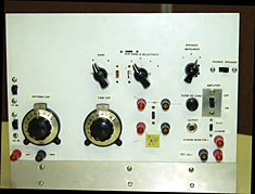
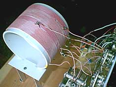
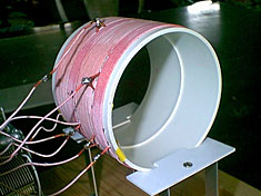
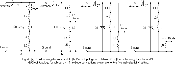
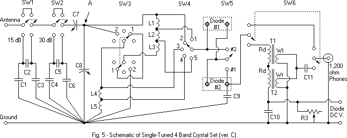
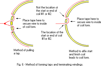
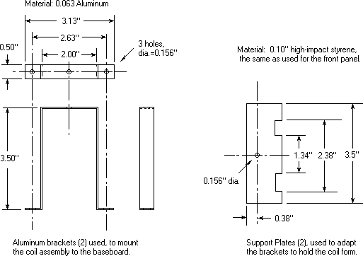
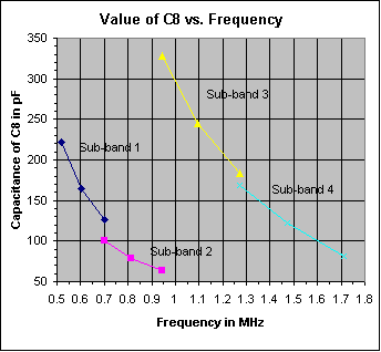
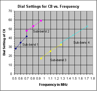
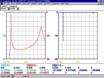
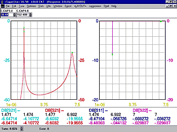
|
Measurement of the sensitivity of a crystal radio set when tuned to a fixed weak signal, as a function of the parameters of the detector diode; including output measurements on 15 diodes Summary: This Article shows how the 'weak signal' power loss, from the resultant operation in the square-law region of the detector, of a crystal radio set, varies as a function of the parameters of the diode used. The measurements clearly shown how 'weak signal' detector loss is reduced when diodes having lower values of the product of saturation current and ideality factor are used. This results in obtaining greater volume from weak signals. Actual measurements compare closely to those predicted from equation #5, developed in Article #15A. It is assumed that the input and output impedances of the detector are reasonably well matched.
1. The Measurements: The measurements of output power are made using a simpler and quicker method than that used in Article #11, since a CW instead of a modulated signal is used. This method involves measuring DC output voltage into a resistive load when the input of the detector is fed from a fixed source of available RF power. A 3.2nW (-84.95 dBW) un-modulated source of available RF power of is applied to the diode for all measurements. This power level is about 12 dB below the LSLCP(i) of the average diode used in these tests. An AM broadcast signal of this power level will result in quite a weak sound in SP phones impedance matched to the output of a crystal radio set. The RF input power is applied through the AMCS described in Article 11. If the input to it is monitored by a DVM connected to the "T" connector, the AMCS should be considered to be an attenuator having an input resistance of 50 and an output resistance of 30.244 ohms. Its attenuation is 22.975 dB. The crystal radio set used in these measurements is described in Article #26. It was used because its performance has been well characterized and its input impedance can be changed over a wide range. The output resistor into which the output power is dissipated is R3. The primary windings of T1 and T2 are shorted when taking measurements. The measurement procedure, for each diode, consists of applying an RF power source having an available power of 3.2 nW to the diode detector, adjusting the input impedance transformation (C7 and C8 in the crystal radio set described in Article #27) for maximum output voltage and recording that value.
The input conditioning device (AMCS), used to aid in measurement of input power is shown in Fig. 2 of Article #11. There, it was used in a procedure to measure input AM sideband and output audio power. Here it is used as a convenient way to provide an accurate source voltage having a known internal resistance. A CW signal generator tuned to, say, 1 MHz is connected to the AMCS as the source of RF power. If the generator has an AM modulation capability, that can be used with headphones as an aid in initially tuning the crystal radio set to the test signal. Table 2 and Fig. 2 show the results of the measurements.
* Is and n were measured using forward voltages of 39 and 55 mV (average current of between 3.8 to 5 times Is).
* Diode load is equal to Rx, its axis-crossing resistance
The red data points indicate actual measurements, the blue, values calculated from equation #5 in Article #15A. The blue line is a connection of points calculated from equation #5. Discussion: Fig. 2 shows the close correlation of measured output power with measured diode n*Is, as predicted by equation #5 in Article #15A. This suggests that n*Is is a valid 'figure of merit' for a diode used to detect weak signals. Remember: The detector power loss figures shown in the last column of Table 2 would be even larger if the test signal of 3.2 nW were smaller. The assumption in all of this is that both the input and output ports of the crystal radio set are reasonably well impedance matched. Note that the input and output resistances of a diode detector using diodes #10 and 11 are very high. Matched input source and output load resistances this high are hard to achieve in a low loss manner. A low loss high input resistive source is easier to achieve with a high Q loop driven crystal radio set that uses the loop as the tank than with one driven by an external antenna and ground that uses a separate high Q tank coil. This is because one of the sources of loaded tank resistive loss, the external antenna-ground system resistance, is eliminated. The radiation resistance of the loop is usually negligibly small compared to the loss in the loop when considered as a stand alone inductor. It is assumed in this discussion that the diode is connected to the top of the loop, the point of highest source impedance. Don't take this as a recommendation to go to a loop antenna for the best weak signal reception. A good outside antenna-ground system will outperform a loop by picking up more signal power. Conclusion: A diode with the lowest n*Is may be theoretically the best, but achieving impedance matching of input and output may not be possible. In practice, a compromise must be struck between a diode with the lowest n*Is and one having a lower axis-crossing resistance (Rxc). This means, in general, a higher Is. It can be achieved by paralleling several diodes or using a different diode type. A good diode array to try in high performance crystal radio sets intended for weak signal reception is an Agilent HSMS-286L, with all three diodes connected in parallel. This diode array is packaged in a small SOT-363 SMD package but is easy to use even without a surfboard to aid in its connection. The three anode leads exit from one side of the package with the three cathode leads from the other. A quick connection solder blobbing all three anodes together and to a thin wire, and a similar connection to the cathodes is easy to do. Use a low temperature soldering iron and as little heat as possible to avoid injuring the diodes. This triple diode performs about the same as six Agilent 5082-2835 diodes in parallel, except that audio distortion will come in sooner on strong signals, because of its low reverse breakdown volt age. It performs best if used in a crystal radio set having RF source and audio load resistances of about 400k ohms, rather high values. An excellent diode for both weak and strong signal reception is the obsolete ITT FO-215 germanium diode, still available, think from Dave Schmarder at http://www.1n34a.com/catalog/index.htm . Crstal radio sets having RF source and audio load resistances of about 200k ohms may have better sensitivity with two of the HSMS-286L arrays in parallel. One section of the Infineon BAT62-08S triple diode should work the same as two HSMS-286L arrays in parallel. Agilent semiconductors are carried by Newark Electronics and Arrow Electronics, among others. Agilent or Infineon may sometimes send free samples to experimenters who ask for them. The apparent error in output power for diode #1 has been checked many times. The figure appears to be accurate. I don't know the reason for the anomaly, except that the diode probably has an increased value for n*Is at the 21 Na rectified current, compared to the value of Is*n from the measurements in Table 1 (made at a higher current). It is known that there are extra causes for conduction in a diode beyond those modeled by the Shockley equation. Other measurements show that this diode also does not follow the Shockley diode equation at high currents (see Article #16). Diodes A, B and C are randomly selected 1N56 germanium units. They also show poorer performance than would be expected from Schottky diodes of the same Is and n. Note that germanium diodes diodes #1, A, B and C provide less output than would be expected from Equation #5. The output from germanium diode #5 is close to that expected from Equation #5 as is the output from all the Schottky diodes. Two charts are presented in Article #16 showing measurements of Is and n for 10 different diodes. The Schottky diodes seem to have fairly constant values of Is and n as a function of current. The silicon p-n junction and germanium measurements show how Is and n can vary, in other diode types, as a function of current. Appendix: The objective of these measurements is to measure the performance of various diodes when used as detectors; at a signal level well below their LSLCP so that their weak signal performance can be compared. The measurements described in this Article were made with an 'available RF power' of -84.95 dBW (3.2 nW) applied to the diode. Here is how that value was chosen: Initial measurements were made using a Tektronix model T922 scope having a maximum sensitivity of 2 mV/cm. The scope was connected to P1 in Fig. 1; the horizontal sweep rate was set to display about 3 cycles of RF. The RF voltage that could be read on the scope, with reasonable precision, was considered to be about 2 mV minimum peak-to-peak, providing a vertical display of 1 cm. The voltage at P1 drives a 25 ohm resistor, the resistance of which is transformed in the crystal radio set up to a value that matches the input resistance of the diode. The correct input impedance match is attained by interactively adjusting C7 and C8 on the crystal radio set to maximize the rectified DC output voltage. 2 mV pp RF voltage equates to 2/(sqrt8) mV RMS. Since available power=Pa=(Erms^2)/(4*source resistance), Pa=5 nW. If one allows for about 2 dB loss between the input to the crystal radio set and that to the diode, the available power that actually reaches the diode becomes about 3.2 nW. To obtain better measurement precision a Fluke model 8920A true RMS RF digital voltmeter was connected to the "T" connector in Fig. 1 and used in the final measurements. Since there were internal noise issues with the Fluke, the 20 dB attenuator (SW3) in the AMCS was switched in to enable increasing the signal to the DVM by 20 dB to overcome the noise. The resistor values in the "inverted L" pad in the AMCS (45.0 and 5.55 ohms), along with the 25 ohm resistor, provide a source resistance of about 30 ohms and an attenuation of 22.98 dB, exclusive of any attenuation introduced by SW1, SW2 or SW3. At first an HP model 3312A function generator was used as the RF source. Final measurements quoted were made using an HP model 33120A synthesized signal generator. Measurements of the diodes having the lower values of Is were made at 892 kHz (Band A, sub-band 1 of the crystal radio set). Insufficient impedance transformation range was available to match diodes having the higher values of Is, so those were measured at 1205 kHz (Band B, sub-band 3). These frequencies were chosen so as to eliminate signal pickup from local stations. The actual insertion power loss in the crystal radio set caused by losses in its L and C components was accounted for in each diode measurement by feeding an RF signal of -84.95+20.98+20+X dBW into the AMCS. (The raw internal power loss in the AMCS is 22.98 dB, and the 20 dB attenuator (SW3) was activated). X represents the L/C losses from the tank inductor and C7 and C8 in the crystal radio set used for the tests. Its value was determined from a computer simulation of the crystal radio set, using a source resistance of 30 ohms and a load resistance equal to the Rxc of the diode to be tested, and noting the insertion power loss as X. The value of X varied from 0.378 dB for diode #1 up to 1.711 dB for diode #11. The simulated crystal radio set consisted of two impedance-matching/tuning capacitors (C7 and C8 in Article #26) with a tank inductor having a Q value extrapolated from the values given in Table 4 of Article #26. The simulation program was 'SuperStar', by Eagleware. Those uncomfortable with the concept of 'Available Power' may find Part 3 in Article #0 helpful. Note that the diodes having the lowest n*Is value (and the lowest detector loss) result in the greatest loss from the tuning components in the crystal radio set. This means that to gain the greatest benefit from using a diode having a low n*Is, the parallel resonant loss resistance of the tank circuit must be made as high as possible(unfortunately reducing selectivity). Note re diode performance when receiving strong signals: A high diode reverse breakdown voltage is important in this case to prevent tank resistive loading by diode reverse conduction dusing the high reverse voltage present during the non-forward-conduction half-cycle. When this happens, volume is reduced. Diodes that have a high reverse breakdown voltage rating usually have a high value for the product of their saturation current and ideality factor and are best for obtaining maximum volune on strong stations. The diodes that are best for weak signal reception usually have a low n*Is product. Many of those who use the HP 5082-2835 report inferior volume on strong stations. I believe the cause is explained above. One solution to this problem is to provide switching means for two diodes as is done in the crystal set described in Article #26. Another possible approach might be to to use several HP 5082-2800 figh-reverse-breakdown-voltage diodes in parallel. Several diodes would probably be needed because of the low saturation current of one '2800. One could also use only one '2800 and supply a little forward bias voltage to make it simulate several in parallel. These approaches have not been experimentally investigated. |
|||||||||||||||||||||||||||||||||||||||||||||||||||||||||||||||||||||||||||||||||||||||||||||||||||||||||||||||||||||||||||||||||||||||||||||||||||||||||||||||||||||||||||||||||||||||||||||||||||||||||||||||||||||||||||||||||||||
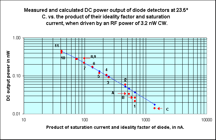
|
How to reduce diode detector weak signal insertion-power-loss to less than that possible when the input is impedance matched Quick Summary: Diode detector insertion power loss can be reduced below the value achieved under impedance matched conditions provided it is operating below its LSLC point. The optimal conditions are: (1) The output audio load resistance equals twice the RF source resistance. (2) The Saturation Current and Ideality Factor of the diode are such that the very-low-signal output resistance of the detector (axis-crossing resistance, aka Rd, of the diode) equals the output load resistance. These conditions insure an impedance match at the audio output and a 1:2 mismatch at the RF input (source resistance = half the RF input resistance of the diode). Please bear in mind that the LSLC point is a point on a graph of output DC power vs input RF power of a diode detector system. It is not a point on a graph of DC current vs voltage of a diode. Info on the LSLC point is available in Article #15a. It has usually been assumed by myself and others that
power loss in a two port device (here, a crystal set) is minimized when
its input and output ports are impedance matched. This article will
show that this is not true in the case of a diode detector
operating at a signal power level well below that of its region
of essentially linear operation. It is true, however, when a
strong signal (well above the LSLC point) is being received. In the
linear region, audio output power is proportional to RF input power.
That is, for every dB of change in input power there will be one dB
change of output power. In the lower power region, called the 'square
law' region, a change of one dB in input power results in a two dB
change in output power. See Article #15a, Figs. 2 and 3 for info on the
LSLC point of a diode detector. Definition of terms: Rd: Resistance of a diode at its axis crossing. Rd=0.0257*n/Is at 25 degrees Celsius
It has been asserted in these Articles that the RF input and audio output resistances, Ri and Ro, of a diode detector, approach the same value and equal 0.0257*n/Is = Rd ohms at room temperature when the input signal strength is low enough. See Article #0, part 4, Article 4, part 2 and Article 16 for information on Is and n, and ways of measuring them. Fig. 1 represents a conventional diode detector. The tank circuit T is shown with no internal loss. A real world tank will have loss that can be represented by a shunt resistor connected across it. For convenience of analysis it is assumed that this loss resistance is absorbed into the source V1, R1 (For a more complete explanation, see Article #1, first paragraph after the third schematic.). Assume that the impedance of the source (antenna) and load (headphone) are transformed to equal values (R1 = R2) and select a diode that has an Rd equal to them. This will result in a reasonable impedance match at both the input and output if the signal power level places operation below +10 dB of the linear-to-square law crossover point. Little of the input power directed towards the detector will be reflected back to the source and most all of the output power from the detector will be absorbed in the load, R2. If the diode detector were a linear device with linear input and output resistances, this impedance-matched condition would result in the least detector power loss (greatest sensitivity) obtainable. It would seem clear that the crystal set detector could not be made more sensitive. Actually, not so! Very weak signal sensitivity can be improved by about 2 dB by appropriate mismatching at the input. This provides a rather hard-to-hear increase in volume, but every little bit helps. In the impedance matched condition discussed so far, R1=Ri=Rd
and R2= Ro. Simple math shows that the detector input voltage Vi will
equal one half the internal source voltage V1. If we create an
impedance mismatch between the source resistance R1 and the detector
input resistance Ri by replacing the diode D with a different one having
1/2 the saturation current, Vi will increase. The reason is that the
detector input resistance Ri is now twice R1. The voltage divider made
up of R1 and Ri will reduce Vi to only two thirds of V1, making
the new value of Vi=4/3 the old value. Since the detector is operating
in square law mode, the internal source voltage in the detector that
drives its output terminals will be (4/3)^2=1.77... times as much as
before. This higher voltage will be divided down by the voltage divider
action of the now twice-as-large diode output resistance and R2 to give
an output voltage 1.185 as large as before. This equates to an output
power 1.476 dB greater than in the original impedance matched condition.
Theoretical calculation and SPICE simulation show that that in a crystal set having equal values for R1 and R2, the diode parameters that give to lowest insertion power loss at low signal power levels fits the equation: R1=R2=2*(0.0257*n/Is) at room temperature. Now let us look at the effect on Ri and insertion power loss if Ri does not match R1. Look at Fig. 2.
Practically speaking, what does all this mean? Mainly, improved theoretical understanding of diode detectors. (see bullet point #4)
|
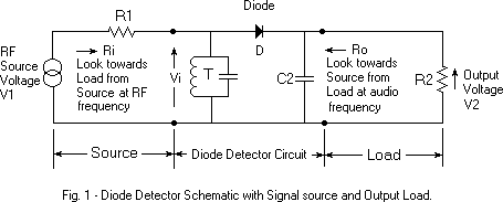
|
About Maximizing the Q of solenoid
inductors that use ferrite rod cores, including charts of magnetic
flux density and flux lines, with some actual Q and inductance
measurements and simulations in FEMM Summary: Many factors interact to affect the Q of ferrite rod cored inductors. Part one of this Article identifies and comments upon some of them. A simplified model and an equivalent circuit is also discussed. The second part describes several ferrite cored inductors, along with measurements of inductance and Q. The third part displays graphs of flux density, flux lines, inductance and Q of several ferrite cored inductors. The fourth part shows how Q varies when the ratio of the length of the solenoid to the core changes Also shown is a chart showing the change of Q when the conductor spacing is changed. The fifth part discusses important info about ferrite 61 and similar materials. Part 1: Modeling of ferrite cored inductors Bulk factors that affect inductor Q:
A simplified equivalent circuit for a ferrite cored inductor is shown in Fig.1.
The simplified equivalent circuit shown in Fig.1 provides a convenient way of think about the effect of placing a ferrite core in a solenoid. Ra and La represent the resistive loss and inductance of the air-cored solenoid without the core (we want to increase the resultant Q and inductance). Adding a core creates the effect of adding a parallel RL in series with the air coil. The value of Lp is equal to La*µi*(LFEM) Henrys. The value of Rp is LFEM*La*ω/CLF ohms. When a core is inserted into the air-cored solenoid, the series resistance of the solenoid in air, Ra, is increased by the factor (FDF-1) to account for the increased power loss in the copper wire caused by the increased flux density from the core. The amount, or percentage of total magnetic flux that penetrates the copper wire is important, as mentioned above. Magnetic flux density surrounding the conductor is not uniform along the length of the solenoid. It is greater at the ends than along its central part. Increasing the length/diameter of the solenoid reduces the percentage of total flux that penetrates the copper and thus reduces resistive copper losses (especially at the two ends of the winding). Increasing the ratio of the length of the ferrite rod to that of the solenoid further reduces the percentage of total flux that penetrates the copper, further reducing resistive losses.
The amount of electric field that
penetrates the core is important, especially at the high end of
the band . The Nickel/Zinc cores such as type 61 have a
very high resistivity dielectric as well as a rather low
dielectric constant (ε) that has a high dielectric loss
tangent (tan δ): Losses caused
by the high (tan δ) may be
minimized by using construction methods that keep the
parts of the solenoid that are at a high electrical potential
spaced away from the core. For instance a coil former sleeve
made of low loss, low dielectric constant material can be used
to isolate the high impedance parts of the solenoid from the
core.
I-squared-R resistive power loss in the conductor caused by the normal current flow: Series resistance of the solenoid reduces Q, especially at the low end of the band compared to the high end, since the inductive reactance is at a minimum there (if the resistance, as a function of frequency is constant). Proximity and skin effect losses increase the RF resistance of the conductor at the high end of the band more than at the low end. The use of litz wire reduces the loss across the band, but more so at the high end. If solid wire is used, spaced-turns winding will reduce the proximity effect losses. An advantage of using Litz wire in a ferrite-rod inductor is that there seems to be no downside to Q from close winding. This helps with obtaining a larger inductance with a smaller solenoid and ferrite core. The use of larger diameter wire to reduce one of these losses usually has the effect of requiring a larger solenoid and ferrite core in order to keep the inductance the same, requiring mind-numbing tradeoffs. Experimentation with 4" long by 1/2" diameter ferrite 61 rods and litz wire of 50/46, 125/46, 270/46 and 420/46 construction with an inductance 250 uH suggest that a winding length of about 1.5" of close-wound 125/46 litz wire is close to optimum, from the standpoint of Q. I've tried to use 660/46 litz with a 4"x1/2" ferrite 61 rod to attain a high Q inductance of about 250 uH. It never worked, probably because the length of the rod, being close to that of the solenoid, caused a high flux density condition to occur near the ends of the solenoid, creating extra copper loss. Ferrite cores of the same specification often exhibit rather wide variations in their ferrite loss-factor (thus affecting the attainable Q when used as a core). They also vary, to a lesser degree, in initial permeability (µi). This affects the inductance. Generally, when selecting cores from a group having identical specifications, the ones with the least initial permeability will have the least hysteresis loss, especially at high frequencies. This provides a convenient way to select cores that will yield the highest Q coils, without actually measuring Q: Wind a solenoid on a thin walled, low loss form and measure its inductance after placing each core, in succession, centered in the coil. Generally the core providing the least inductance will provide the highest Q. Comments: Consider the
schematic in Fig.1. La, Ra and Ra*(FDF-1) define the inductance and
Q of the air-cored solenoid (Before a ferrite core is inserted in an
air-cored solenoid, FDF=1). Summary: With no ferrite core present one has, of course, a low Q low inductance inductor. If one could construct a fully flux-coupled ferrite 61 core (LFEM~1.0), the Q at 1 MHz would be 1/ui*CLF=267. Highest Q occurs with an optimum value of LFEM, which also provides an intermediate value for real-world inductance. See Table 6, next to last entry. In my experience with 1/2" diameter ferrite 61 rods aiming for 250 uH and using Litz wire, most of the time LFEM turns out to be greater than the value for maximum Q. An indication of this condition can be obtained by placing two extra cores, each co-axially aligned with the solenoid's core, one at each end of said core, to increase the LFEM. The Q is usually reduced even though the inductance is increased, showing that LFEM is too high for maximum Q. Proof of this can be attained by discarding the two extra cores and reducing the number of turns on the rod. Of course, inductance goes down, but Q will increase. To get the inductance back up and retain the higher Q, a solenoid and ferrite rod of larger diameter are required. An un-tested opinion: A solid ferrite rod inductor having a specific diameter D will have a better Q than if many small diameter rods were used to fill up the space of the specific rod. One solid rod with a diameter D that has a central axial hole should work about as well as the solid rod if the hole is not too large, say a diameter of D/3 or D/2. This is because most of the magnetic flux, radially speaking, is not spread uniformly across the circular area of the rod, but concentrates nearer to the surface. This means that even if the multi- core has the same total ferrite cross-section as the single-hole core, the single-hole core should provide a better Q than the multi-rod core. ** Note the "no core" entry in Table 6 for inductor BB. The solenoid (with no core) has a Q of 88 (and an inductance of 17.6 uH).
Part 2: Measurements
Comparison of several conventionally wound Ferrite-cored solenoids having the same winding length and number of turns, but different diameters Ferrite rod length=4", diameter=0.5", material=type 61, µi=125, ferrite loss factor (CLF)=30*10^-6, the "best ferrite core" was used, former=low loss thin wall tubing of various lengths, wire=125 /46 ga. litz, construction=conventional close wound solenoid of 58 turns having a length of about 1.625".
* Piece of polyethylene tubing having an OD of
0.625" and an ID of 0.50" Some observations:
Comparison between a conventional and contra-wound ferrite-rod cored solenoid using a "best" and a "worst" rod.
Ferrite rod length=4", Diameter=0.5", Material=type 61, µi=125,
Ferrite loss factor (CLF)=30*10^-6, Former=polyethylene (not
vinyl) tubing, ID=0.5", OD=0.625", length=5", Wire=125 strand/46
ga. litz, Construction=close-wound conventional solenoid of 58
turns having a length of about 1.625"
Ferrite rod length=4", Diameter=0.5", Material=type 61, µi=125, Ferrite loss factor (FEF)=30*10^-6, Former=polyethylene (not vinyl) tubing, ID=0.5", OD=0.625", length=5", Wire=125/46 ga. litz, Construction=close-wound contra-wound solenoid of 58 turns and length of 1.625" (not wound as tightly as the conventional solenoid above).
The winding format for solenoids #1 and #2, below, are shown in Figs. #2 and #3 above. For clarity, the windings are shown as space wound, but the actual solenoids #1 and 2 close wound. Connections for the contra-wound inductor shown in Fig. 3: For the series connection, join leads c and e. Lead d is hot and lead f is cold. For the parallel connection, join leads c and f. Join leads d and e. d/e is the hot and c/f is the cold connection.
The Q values given above were measured on an HP 4342A Q meter and corrected for the distributed capacity of the inductor (Co). The ferrite cores were purchased from CWS ByteMark in the third quarter of 2002. They may have changed vendors since then because some rods I purchased in the 3td quarter of 2004 resulted in lower Q coils than the values reported here. The rods also had two small, 180 degree apart, longitudinal flats along their entire length. CWS gracefully accepted a return of those rods and quickly refunded my money. The 'best' and 'worst' cores used in these measurements were from a group purchased from CWS ByteMark in the 3rd quarter of 2002. Note the better high-band Q values recorded for the contra-wound inductor. This is because the low Q distributed capacity from the dielectric of the ferrite (Co and Ro) is connected across an inductor having 1/4 the inductance (and reactance) value of the conventional wound solenoid. An observation: If the hot/cold connections to the contra-wound coil in Fig. 3 are reversed, Q at 1710 kHz drops. This is because more loss from the low Q dielectric of the ferrite is coupled in to the stray capacitance. Solid wire instead of litz?: Keep in mind that the work described here used close-wound 125/46 litz wire. If one duplicates 'Coil and Former B' in Table 2, except using 22 ga. solid copper wire (having the same diameter) as 125/46 litz, the Q values drop to about 1/6 of the values achieved with the litz wire. The cause is the large proximity effect resistive losses in the solid wire. The proximity effect, but not the skin effect loss may be much reduced if the wires are space-wound. New trade-offs now must be considered: Same wire diameter, and therefore a longer solenoid, or a smaller wire diameter and the same overall length? If one wishes to use solid wire, it should probably be wound directly on the ferrite, not on a former. The overall Q will still be much less than when using litz, but the loss from the high (tan δ) dielectric of the ferrite will be pretty well swamped out because of the now higher losses from the skin and proximity effect losses. The Q values, using a close-wound solenoid of 22 ga. solid copper wire on a polyethylene former, as in 'Coil and Former' B in Table 2 are: 520 kHz: 130, 943 kHz: 141 and 1710 kHz: 150 when using the "best core". The Q drops only 3, 3, and 5 points respectively if the "worst core" is used. Measurements to determine the (tan
δ) of the dielectric of a 'medium core':
Two copper foil coupons, 0.5"x1.75" were affixed to the 4", 0.5"
diameter rod made of material 61. The long dimension of each coupon
was parallel to the axis of the rod with the two coupons set
opposite to each other, 180 degrees apart. They formed a two plate
capacitor having curved plates with the dielectric of the rod
between them. The capacitance of this capacitor came out to be 6.5
pF. Measurements, using a Q meter and a high Q inductor were made
that enabled calculation of the Q of this 6.5 pF capacitor. Q was 25
at 520 kHz, 35 at 943 kHz and 55 at 1710 kHz. Even though the
distributed capacity of a ferrite rod inductor is only made up
partially of this poor dielectric, it is, I believe, a previously
unrecognized cause of the usual Q drop at the high end of the band.
It is also, I believe, the cause of Q reduction in ferrite
toroids when no gap is provided between the start and finish of
the winding. Part 3 - Flux density and flux line Simulations, inductance and Q of several ferrite cored inductors along with the measurement of one inductor The FEMM (Finite Element Method Magnetics) program was used to generate Figs.1-8. First a word about the displays: FEMM, as used here provides a 2-dimensional display of flux density (the colors) and flux lines (the black lines). Only half of the object being simulated is analyzed and displayed since only axis-symetric objects can be analyzed with the program. This saves simulation time, which can become very great. FEMM, at this time, cannot simulate using litz wire. That is why the following simulations and measurements use 22 ga. solid copper wire instead of the 125/46 litz used in Part 2. Fig. 1 is a plot of the flux density and flux lines on an imaginary plane that cuts longitudinally through the center of a he ferrite rod-cored inductor, shown mostly in purple. The outline of the 4"x1/2" rod is shown at the left of the plot. If one measures, on the computer screen, the height and width of the rectangle, one can see that their ratio is 16. This is equal to the ratio of the 4" length of the rod to 1/2 of its 1/2" diameter. The large half-circle defines the area around the inductor that will be included in the simulation. It's made up mostly of air. The magnitude of the flux density can be seen from the colors on the display (see the chart). The range of flux density values for the display was purposely limited to about 20 to help supply flux density detail around the outer turns of the solenoid. That is why most all the core is colored purple (the flux density is above 4.000e-9 Tesla). Fig. 2 is a close-up simulation of the area near the upper turns of the solenoid. If one's browser has a zoom control, one can easily see how the flux density close to the surface of the wires of the end turns of the solenoid (even numbered Figs.) is greater than it is in the more central turns. High flux density in the copper equals high power loss (Q reduction). Comment: Look at figs. 3 and 7 in Table 4. Inductors BB and EE are identical except for the length of the ferrite rod. It appears that about 10% of the end turns of solenoid BB are exposed to a flux density above 2.8e-9 Tesla (3 dB below the maximum plotted value of 4e-9 T). The corresponding percentage in solenoid EE about 50%. This shows that a high flux density around a greater percentage of turns results in lower Q. A parameter listing of the inductors is below Table 4. Note the Q values for inductors BB and EE.
Parameters of simulated inductors AA through DD, inductance and Q at 1 MHz:
Note that the Q difference between the "Best core" and the 'Worst core" is very small. This is because the main loss in this inductor is the high proximity loss in the solid close-spaced copper winding. The much lower ferrite core loss is swamped out and has little effect on Q, showing a Q ratio between the two of about 0.97. Compare these figures with those in Table 3 for a similar conventionally wound solenoid using close-spaced 125/46 litz wire. Proximity loss is greatly reduced in close-wound litz wire, compared to close-wound solid copper wire. The Q ratio here is about 0.75. Loss in the ferrite core swamps out the much lower proximity loss in the litz wire, and a much higher Q results. Part 4 - Ferrite-rod inductor simulation experiments; all using centered solenoids 1.624" long and having 58 turns The solenoids used in the simulations in Table 6 all use a conductor having a diameter of 0.0253". The only parameter varied is the core length. The simulations in Table 7 all use a 4" long core. The only parameter varied is the diameter of the conductor.
* Solenoid winding covers the full length of the core. Table 6 shows that about 77% of the maximum Q is attained with a core about 2.4 times the length of the solenoid. About 68% of the maximum inductance is attained. Note also that when the length of the core is shortened to approximately the length of the solenoid, Q drops precipitously. Resistive losses are mainly proximity effect losses. Hysteresis losses are magnetic losses in the ferrite core itself. Total losses are the sum of the two. There is a good lesson to be learned here: To maximize Q, do not cover the whole length of the core with the solenoid.
* Simulates winding the 58 turn solenoid directly on the 4" long ferrite core (solenoid ID=0.5013") instead of on a former having an ID of0.6263". Note that the the two simulations using a conductor diameter of 0.008995" show remarkably similar parameter values. Table 7 shows the benefits of space winding when using solid wire. All the inductors in Table 7 use centered have solenoids of 58 turns and a length of 1.624". The only variable is the diameter of the conductor, which controls the spacing of the turns (the winding pitch is held constant). The lesson here is that, when using solid copper wire, there can be a great Q benefit by space winding the solenoid, using an optimum size wire, in this case a Q of 431.9 vs 130.1 at 1 MHz. See Table 3 for measured inductance and Q values of an inductor similar to inductor BB, but wound with 125/46 litz wire. Here the Q is even greater than in Table 7 because litz construction is less sensitive to proximity and skin effect losses than is solid wire. Thanks must go to Brian Hawes for making me
aware of the FEMM program and showing me how to use it. Part 5: Perminvar ferrite, and what the term means Normal nickel/zinc ferrites (NiZn), the types with less permeability as well as lower loss factors than manganese/zinc (MnZn) ferrites, are often used at RF because of their low loss at the higher frequencies. They do not suffer appreciably from permanent changes in permeability or loss factor from exposure to strong magnetic fields or mechanical shock such as grinding, or dropping on the floor. Special nickel/zinc ferrites, called perminvar ferrites can achieve a considerably lower loss factor for the same permeability than normal nickel/zinc ferrites, and at higher frequencies. This result is achieved by adding a small amount of cobalt to the ferrite power before firing, but there is a catch. In order to actually achieve the lower loss factor, the ferrite core must be annealed by raising it to a temperature above its Curie temperature (the temperature at which it losses all its permeability), and then cooling it very slowly back down through the Curie temperature, and then to lower temperatures. This process usually takes about 24 hours. The Curie temperature of ferrite type 61 (a perminvar ferrite) is specified in the Fair-Rite catalog as being above 350 degrees C. The annealing process reduces the permeability somewhat, but reduces the loss factor substantially. The low loss-factor property of the annealed perminvar ferrite can be easily degraded by mechanical shock, magnetic shock or just physical stress (as from a tight mounting clamp). The Fair-Rite catalog sheet for type 61 ferrite cautions "Strong magnetic fields or excessive mechanical stresses may result in irreversible changes in permeability and losses". Actually, the changes are reversible if one goes through the annealing process again. The MMG catalog, issue 1A, in writing about perminvar ferrites, adds: "Mechanical stresses such as grinding and ultrasonic cleaning increase the permeability and lower the Q, especially at the higher frequencies, although the changes in Q at the lower frequencies may be very small. I suspect that there is now much less pressure on
ferrite manufacturers to deliver a low loss product than in the
past. Since time is money, maybe they now skimp on the annealing
process. Several years ago I took some 4" x 0.5", mix 61 rods I had
purchased from CWS ByteMark and had them re-annealed at the plant of
a local ferrite manufacturer. The Q of a litz-wire coil using the
re-annealed core, at 2.52 MHz, was increased by 12%. This
indicates that the core was not originally properly annealed, or had
been subjected to some mechanical or magnetic shock after being
annealing by the manufacturer. I was informed, when I asked, that
coil Q at high frequencies could be expected to increase by up to100%
from the pre-annealed value. I chose the best of these
re-annealed rods to be my "best ferrite core" rod in this Article. One
source informed me that few ferrite manufacturers perform the
annealing process anymore. Toroids made of type 61 material are
still made here in the USA. |
|||||||||||||||||||||||||||||||||||||||||||||||||||||||||||||||||||||||||||||||||||||||||||||||||||||||||||||||||||||||||||||||||||||||||||||||||||||||||||||||||||||||||||||||||||||||||||||||||||||||||||||||||||||||||||||||||||||||||||||||||||||||||||||||||||||||||||||||||||||||||||||||||||||||||||||||||||||||||||||||||||||||||||||||||||||||||||||||||||||